Yann Guidon / YGDES
-
Carry chain considerations
04/17/2017 at 09:48 • 5 commentsThe incrementer and the ALU are becoming the critical parts of the whole system and the length of the carry chain will affect the operating speed. In itself, the clock speed is not a goal (the thing is already sooo sloooow that you can see it think, which is all the point). However, the faster it runs, the faster it can scan and refresh the memory, which is quit a big deal. If I can manage to get 25IPS (approx 2× faster than the Harvard Mark II), then it still requires 10 seconds to scan 256 words, 1/3 of a minute to refresh the whole 512 words of DRAM. And refresh only happens when the processor doesn't access the memory, a full refresh could last one minute. I haven't yet evaluated the retention time of the DRAM but I feel I'm pushing the design in uncharted territories.
With 100µF capacitance, a 1µA leakage will make a time constant of approximately 100s which, depending on parts tolerance, where the leaks go, the actual rate and current of leakage etc. This is pretty close to the above quoted minute and I'm concerned.
The new instruction register introduces a "latched sensor" which has several interesting benefits but one major consequence over the overal design: the processor is now pipelined, with fetch, execution and DRAM cycles being overlapped. The clock sequencing is pretty simple now : 2 phases, which directly drive the temporary storage caps of the DFF. There is no funky sub-cycles anymore. The complexity is now relegated to the software because data access and jumps are now delayed. I should add a 25th instruction bit to tell the program sequencer to wait for one more cycle until data are available...
The speed is now limited by two main factors:
- the carry chain delay
- the time to fully charge the latching capacitors of the DFF
As I have already examined, the charge time depends on several factors, such as the charging voltage and the series resistance, so they can be somewhat adapted. The carry chain length is however a more structural problem. If a relay switches in 4ms, a chain of 4 relays will need 16ms to propagate, and I would ideally keep it under 20ms. Add to this about 10ms to charge the caps then switch them to the coil, and we have about 30ms of cycle time, or 30Hz.
To reach this speed, the critical datapath must be under 6 relays.
My problem is that the РЭС has a rather low fanout capability and it wouldn't drive 15 coil loads. I guess a reasonable fanout is 4, though I remember I estimated 3 when I started the #SPDT16: 16-bits arithmetic unit with relays project.
Of course, less fanout is better and the LSB relay (bit 0) will take all the heat, vibrations and load so it must be particularly carefully designed (or it might break).
@Tony Robinson has explored a particularly interesting approach: a OR-chain made of diodes that could greatly accelerate the propagation in my case. However the diode drops are significant, let's assume 0.8V for the 1N4148 and this becomes quicly impractical. And the fanout problem is not solved, the first diode will take all the current to drive all the coils in the chain... I could cheat by using high power Schottky diodes though but it wouldn't remove the high current draw when all the chain is ON.
Apparently I am forced to use a segmented approach. Naturally the 16-bits incrementer is split into 4 equally sized segments, but not identical: the LSB have a high fanout while the MSB have a high fanin. I can also mix with a diode here and there to reduce the complexity/size/cost/consumption a bit. With this scheme, the propagation time might drop to 2 coils delay, but the incrementer will use a LOT of relays...
The linear approach is slow, the fast approach (O(n²)) is prohibitive, so a hybrid approach is considered, using 4-bits segments. Hopefully, the fanout is not excessive and the cascade time is 4 coils (in the 16ms range).
I have a drawing in my head, I'll need to refine it...
Update 20170420: I made the pictures !
So it started with the carry chain of Tony Robinson's idea of using diodes to accelerate carry propagation. But this is not adapted for relays. I came up with this version that solves the diode drop problem.
![]()
However this circuit is
- wasteful (a lot of energy is lost in the "balancing" diodes)
- still plagued with the fanout problem (Cin drives up to 5 coils in parallel, or 7 ohms of equivalent load)
So I applied the same recipe as with other parts of the system: when parallel becomes an issue, go serial!
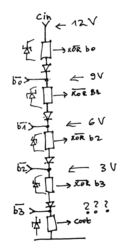
And it looks promising: using a 12V rail, the coils can be connected in series with the diodes. It started like this:
![]()
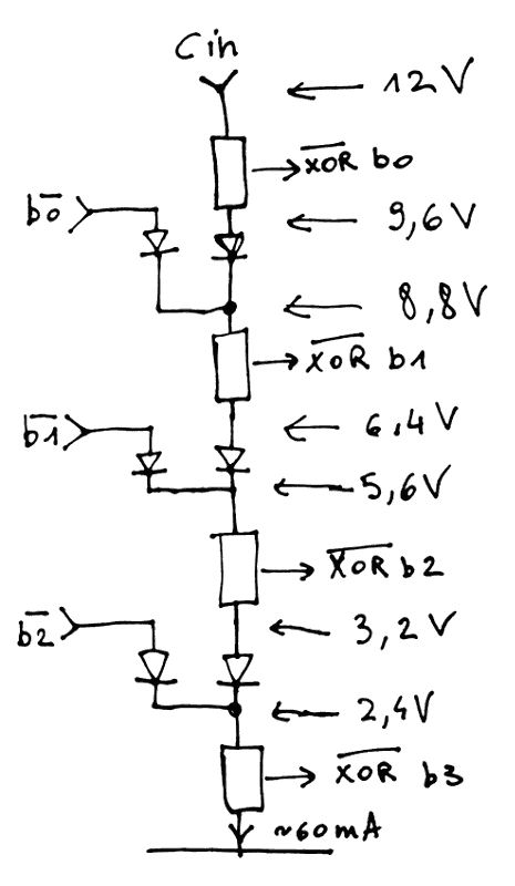
5 relays and 4 diodes in series don't work but it's promising. With only 3 bits and one more relay for the level translation, the voltages look very good:
![]()
This method is energy efficient, even though there is almost always current flowing in most of the chain. Only 2 diodes per bit are used (and almost always dissipating). With the proper voltages, I even wonder if it's possible to get rid of the diodes. But since the voltages fall almost perfectly with the existing rails, I'll keep 4 coils in series.
I'm OK with 3 bits per strings because 16 bits is 3×5 (+1) so the propagation delay is only slightly worse than with 4 bits per string and the design looks reliable and uses few relays.
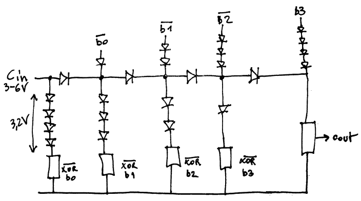
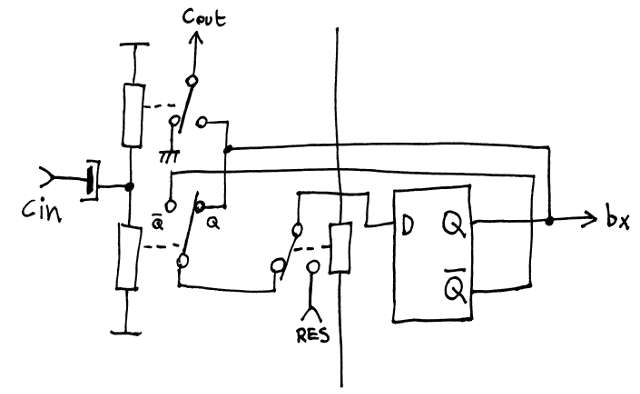
The actual carry chain looks like this:
- b0 is always /b0 so there is nothing to see here.
- the first Cin comes from the inverted b0 and computes b1, b2 and b3 (and Cout)
- then b4, b5, b6 and Cout
- then b7, b8, b9 and Cout
- then b10, b11, b12 and Cout
- then b13, b14, b15 and some error flag ?
The carry chain itself has 4 coils of delay but a 5th coil delay comes from the XOR. Still: 5 coils delay is just what's needed to provide the PC+1 just in time at the end of the cycle.
Mission accomplished? Not so fast! There are 2 new problems...
- How do I generate 9.6V for the 3rd relay ??
- How do I even get the high voltage levels out of the flip-flops ?
...
The additional rail is not hard to get : just use a dumb resistor (typical 39 ohms) tied to +12V. That's overall 5 resistors. There are other rails : 6.6V and 3.3V with perfectly suitable voltage.
I don't like to waste power so I thought about putting a relay coil instead of the resistor but what would it control ? There is no need to try to speed things up because the critical datapath is just right.
The 2nd question is more difficult. The output of PC is 3.3V level, going to the datapath, and also looping back to the DFF. This is good for the bottom of the diode ladder but the two other levels require some sort of level translation. This uses one more relay...
To speed things up, the relay can be in series with the 2 other latch relays but this is not a balanced configuration (the number of relays is odd). A resistor is necessary but a 4th relay might be necessary to drive the PROM address decoders. DPDT relays are soooo handy......
Overall, for each bit of the PC, we have :
- 1 relay to select the source (result or PC+1)
- 1 clock relay (with its capacitor)
- 1 relay for the XOR
- 4 relays for latching and fanout (2×loopback@6V, datapath@3V, PROM@12V ?)
= 7 relays ....... that's about 112 relays for PC, running mainly at 6V, and 32 diodes.
-
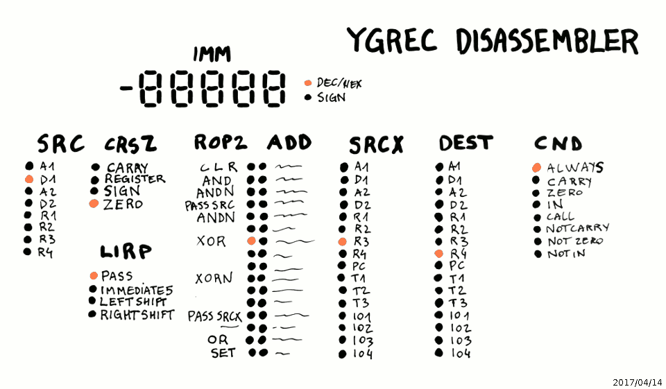
Programming the YGREC
04/14/2017 at 09:17 • 0 commentsSo far the instruction format and datapath are well defined and it's time to think about the programming paradigms used by the YGREC.
The architecture does every important thing (as far as I'm concerned) and I notice that it has no opcode.
That's a bit unusual though it's reminiscent of the "Move Machine" ou "Transfert Triggered Architecture". Where the TTA/MM starts operation when operands are available and there are only 2 register addresses, the YGREC has 3 addresses and the operation is immediate.
How should instructions be written ? There are two schools : the algebraic form (used by ADi DSPs) and the direct form (mapping the hardware fields). I like the ADi style (ah, the memories of the SHARC and ADSP2105)
R1 = D1 or T1 SHR (IFZ)
but it's more coherent to stick to the representation of the hardware assembler board...T1 SHR or D1 => R1 (IFZ)
That's where I see that I should swap the ALU field and the SRCX field on the assember board. Too laaaaate... But I can move the ADD/ROP2 button. You will not notice much.
There, I fixed this :
![]()
The disassembly board must also be swapped :
![]()
So there, you have everything clearly laid out, just write the code and enter each column in order, and you have your instruction in binary !
Almost in the same vein, there is another question : how to encode NOP ?
Starting with the #YASEP Yet Another Small Embedded Processor I set the following convention:
- NOP is all-zeroes.
- INV is all-ones
NOP does nothing so it should be encoded in a way that does not modify the state of any register. Let's see how each field is affected :
- SRC, SRCX, DEST = 0 should not trigger a memory access. For now 0000 points to A1 and it's not good, so let's swap A1/D1/A2/D2 with R1/R2/R3/R4.
- LIRP : should be in PASS mode, R1 is not modified
- CRSZ field : not affected because LIRP=PASS, but let's say 00=ZERO
- ROP2 mode should be either PASS_SRC or PASS_SRCX. However these codes are assigned to 1100 or 1010 so two bits must be inverted...
- The condition could be "NEVER" if there was one anymore so it's "always", so CND=000="always"
- The Imm flag is 0, which says it's a register source
In the end, NOP is equivalent to
R1 PASS R1 => R1
INV however requires a sort of reset of the program. This corresponds to hitting a place in EEPROM that has not been programmed and reads 0xFFFFFF.
- The Imm flag is 1, which says it's a IMM16 source, which is set to 0xFFFF. Let's use this as the address to jump to and restart the program. A sort of implicit jump vector.
- The condition is 111, which is the opposite of ALWAYS. We don't have "NEVER" anymore but we have "CALL" !
- Call is a bit messy because it swaps the destination register. The result (IMM16=0xFFFF) will go directly to the PC while its old (contents+1) is written to the destination register, which is IO4 for now.
Nobody knows what is hooked to this output register and it'd be a shame if something happened there. This is easily solved by swapping the IO and the T quatuors of registers, so PC becomes 1111.
INV is now equivalent to
FFFFh => PC (CALL)
And the new register map is:0 1 2 3 4 5 6 7 8 9 A B C D E F R1 R2 R3 R4 A1 D1 A2 D2 IO1 IO2 IO3 IO4 T1 T2 T3 T4 .
-
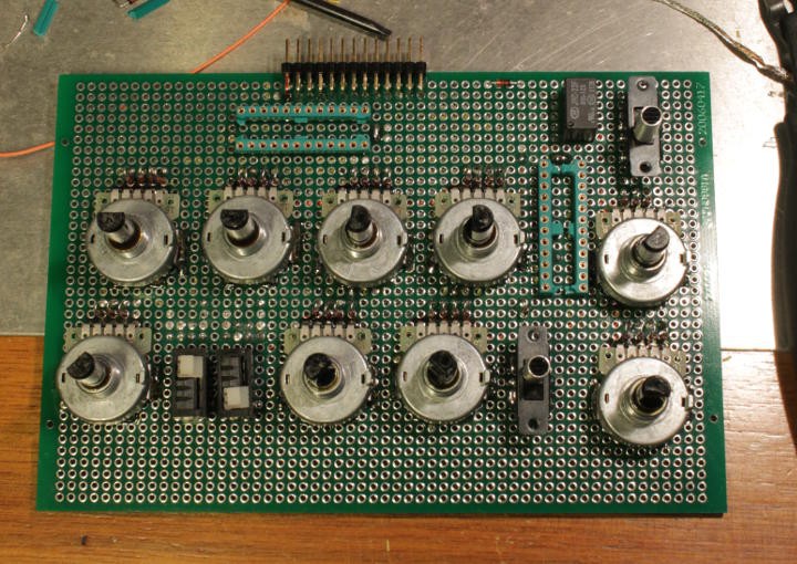
The assembler and the instruction register
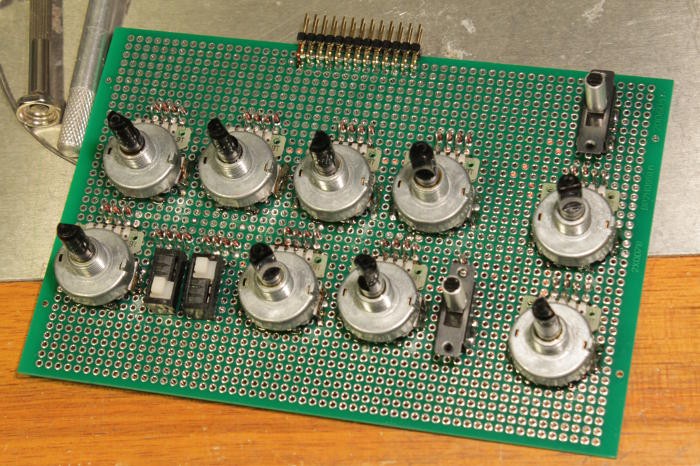
04/14/2017 at 07:24 • 0 commentsI just finished the assembler board !
I had to remove all the diodes and put new ones in the reverse (appropriate) direction.
![]()
I'll need to label the buttons... but it's a hack ;-)
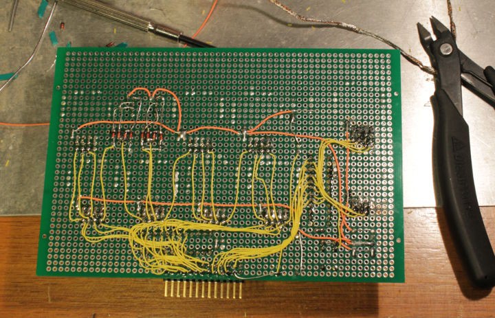
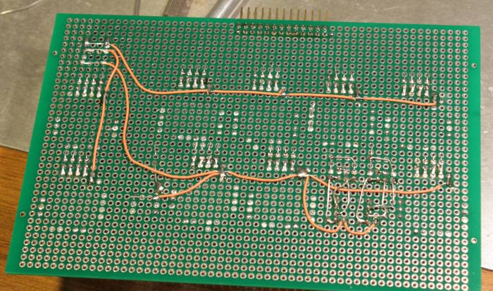
I also wired everything, which makes the other side quite pretty as well :-D
![]()
The shift registers are in parallel with the buttons, they are not completely wired because I'm waiting for their delivery. The 2×16 outputs drive the 24 bits of the instruction as well as disable the switches (through the small relay). 7 outputs are still available for other functions. It looks a bit like a mess because I tried to map the pins to the actual instruction bit number. There's no magic there, I should draw some schematic though. One day.
And after all was said and done, I realised I should have put diodes on the outputs of the shift registers...
Too late, I'll just remove the DIP chips from their sockets when they're not in use :-)
But now I have to test the board and the instruction register's latch. This means, prototyping the 3-relays sensor and latch...
-
How to drive РЭС15 relays with a computer ?
04/13/2017 at 07:18 • 7 commentsThe last log 10. Electromechanical User Interface : the Assembler board raises an interesting and important question : how can I control the relay-based computer with something like a Raspberry Pi ?
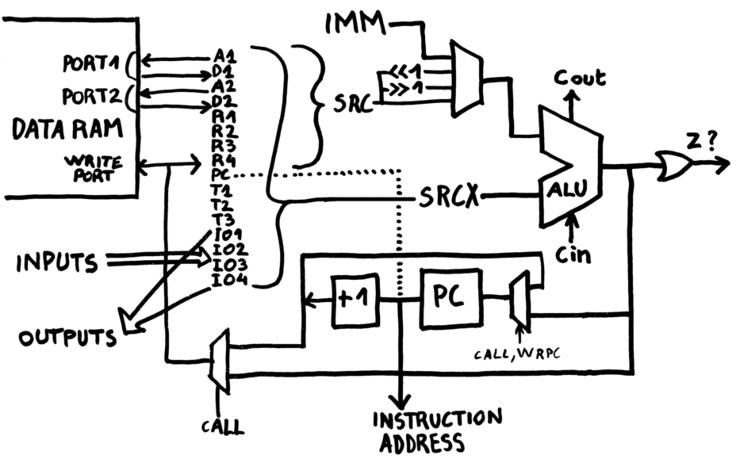
I'd like to control and spy on the machine with a modern computer, replace the DRAM and the PROM with user-controlled modules that emulate them with SRAM, write or read registers, see the result of instructions, upload and save programs...
I need to interface hundreds of signals from a 3-6-12-24V system (requiring 60mA drive currents) with the meek 3.3V CMOS GPIOs of today's generation.
The last log implied that the instruction bus would "switch the high side". I already have the signal distribution paths figured out but I didn't think too much about the most favorable direction of the data signals. I just assumed the sense coils to be wired to 0V and the data coming from +Vcc. Simple.
(diagram)
Then the building of the Assembler board made me reconsider my assumptions because I would like to "upgrade" the board to add a shift register that takes over the switches.
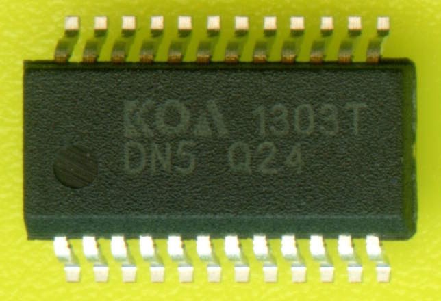
All the practical electronic/IC solutions I could find are referenced to GND and "switch the low side". The sense relays require some significant current (60mA without prebias). In particular, this part is very well suited to the task:
![STP16DP05B1R 16-BIT CONSTANT CURRENT SINK LED DRIVER]()
This obsolete chip is a 16-channel constant-current sink LED driver in 24-pin DIP. It runs up to 20MHz with 3V-5.5V logic supply but can sink up to 80mA per channel (20V maximum on the pins). I need 1 and half to drive the instruction sense relays... From the lower side.
I have already wired the diodes of the switches for high-side, I can change them. But the ROM and PROM boards already have some parts in stock, that are meant for high-side switching !
The solution comes again from exdwh's store !
Isn't this cute ? Inside the KOA DN5Q24T, you'll find 36 diodes !![]()
That's a big jump from the previous 2 diodes per package...![DN5 diode network]()
The even funnier thing is that you can configure it however you want, with low side or high side: just connect the appropriate common rail to the proper voltage. The circuit is also (almost) symmetrical so a single footprint/PCB can accomodate both uses, just solder the package in the appropriate direction ! (ooooops I realise now it's a miroring and not a rotational symmetry)
The leakage is too high and the voltage rating too low to help with DRAM. But if the voltage is kept low enough (less than 7V) this is totally suitable for the PROM boards, as the current is just enough and the spikes shouldn't last long enough to damage the diodes.
Now, I must find a way to increase the sense coils' sensitivity...
The current and voltage can be reduced with a switched capacitor cell which is almost the same circuit as the typical latch.
- The hysteresis is held by 2 coils in series, so there is one output for the datapath control lines, and one for the disassembly board.
- The middle point is tripped by a capacitor, switched by another relay. Just like the latch circuit.
- The other side of the relay is held high by a pull-up to 6V. Value: t=RC, R=t/C, the charge is held in a 100µF capacitor (like most others). It must be charged in 20ms, which gives about 500 ohms. Rounding up to 600 Ohms gives 10mA when shorted to 0V, instead of the 60mA we wanted initially... the added diodes will reduce the current a bit more.
- To increase sensitivity, the sense middle point is held at 3.3V by 2 resistors (on the 0V and 6V rails). In parallel with the resistors, capacitors stabilise the relays...
- The input is held high by the pull-up, but overriden by the low-side switches (either solder blots, switches, N-channel FETs....)
The sense coils become "instruction register" (using no less than 3 caps, 3 relays, 3 resistors).
(diagram)
This is interesting because the capacitor switching can be controlled by the same clock as the register set (when enabled). This creates some pipelining, which makes scheduling more interesting... there is a fetch during exectution.
Very interesting.
-
Electromechanical User Interface : the Assembler board
04/12/2017 at 03:48 • 0 commentsSee log#4: Assembler and disassembler
Try to do that with a x86 !
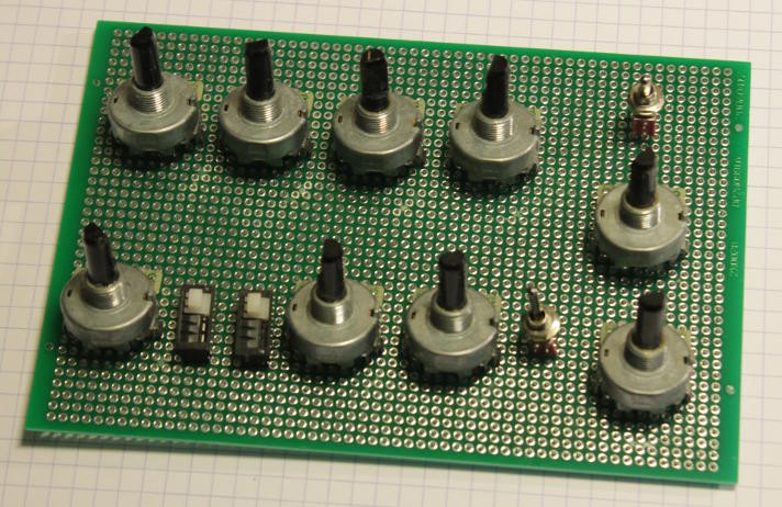
The YGREC's instruction format is so simple that 9 hexadecimal rotary encoders and a few other switches are enough to "assemble" one instruction word. With the help of some diodes, I admit, but nothing crazy and no weird encoding table...
![]()
Luckily I have 4-positions slider switches in stock :-)
There is the question of how to encode the IMM5 field : with the IMM16 or with SRC+CRSW fields ? In either case, a 2-diodes drop is inevitable. However the IMM16 encoders can't be "split" so I Keep It Simple and remain with the SRC+CRSW solution. Simpler and easier though maybe a bit confusing. You'll get used to it ;-)
The switches and diodes are soldered. I have chosen a 26 positions connector for ribbon cable, a handy size to transmit 24 bits of instruction, one supply/enable bit and a key (not implemented).
![]()
![]()
The 4-positions slide switches are encoded to 2 bits with 4 diodes each.
I'd like to test the board while it is being wired but I'll have to wait for the build of the disassembly board.
I notice that I have enough room to add a few DIP chips. I'd easily put some 74HCT595 but they don't provide enough current. Amplifying devices would use much room and need to be "high side". Maybe LED drivers ?
Whatever solution I imagine, the board should sink the current, because the input voltage is unknown. Electronics needs a ground reference. I also have the STP16DP05B1R in mind, a 16-ports constant current sink LED driver, that can get up to 80mA (I need 60-70mA). It's like a dual 74HC595 on steroids.
However I have planned from the beginning to have the sense relays ground-based so a higher voltage is required (at least 3V), and I have already bought the dual-diodes for the ROM matrix, connected in the direction of the grounded coils...
I can spend a bit of time reversing the 40 diodes of the assembler board but the PROM boards will still have the wrong diodes, or require more efforts during soldering...
Unlike the rest of the system, the instruction input is using unipolar signals, with disconnected=0 and 1 is signaled by a pull-up (through diodes). The current and voltage must be enough to trip 2 relays in series because the disassembler board must intercept the instructions.
20170413 : I think I've found the solution, see the next log :-)
-
Flip Dots !
04/11/2017 at 06:32 • 13 commentsWhile rumaging through my stash, looking for electromagnets, guess what I found ?
![]()
Yes, memories from Active Surplus, a now closed Toronto surplus store. Damn, I miss you guys...
4 individual flip dots, 10×10mm, that flip at about 1.5V and 70mA (they are measured at 19.2 ohms).
I might use them for showing status (like Z and C flags) and they are easily interfaced in a CCPBRL way : one leg to 0V, the other leg tied to a capacitor (it worked with 100µF under 3V but 470µ is better) that swings from 0 to 3V... or something like that. Hysteresis is built into the system (through ferrite that stores the magnetic flux) so there is no need to maintain a bias current.
Which makes me think...
Without the need to provide bias, a completely electromechanical calculating machine would need no static/constant power !
-
Tubular bell
04/11/2017 at 04:47 • 5 commentsOh well, this entry is maybe related to the classic piece of the same name.
But the origin goes back to last year's #SPDT16: 16-bits arithmetic unit with relays where I wanted to "ding" a bell when a multiply or divide multi-cycle operation was over.
It turns out that the "bell" I found online was not appropriate. It's an electromechanical oscillating ringer with a nasty sound that lasts as long as you supply it with current. It works but meh.
I want a real bell, a distinct sound that will rise up from the clatter and clickety vibrations of the thousands of relays. Something monotonal and different. But I don't want to bet on a wrong item again on eBay.
Then I remember that video (linked above) and the final minute. Tubular bells. I realise I don't need a "bell" shaped metallic structure, I just need a steel tube !
Well I happen to have some (sold as blinders bars in the decoration shop on the corner) and I just sawed 395mm out of the 16mm diameter rod. There is no special reason for this length, though it sounded ok when I tested the whole bar. The original bar was 2m long, 2m/0.4m=5 so I think I struck the 5th harmonic.
Then it's an easy matter to determine the nicest-sounding vibration mode, and select the best place to "excite" the tube. I pass the tube through a sheet of hard foam and find that it sounds OK when the fixation foam is approximately L/4 (a tiny bit more, probably because the interaction with slightly detuned higher harmonics create a low frequency vibration). "Excitation" comes from the bottom. That's not practical to hang a 40cm tube from the final structure and I would prefer a horizontal system like with vibraphones...
I can use a horizontal configuration by placing the foam at the exact middle of the tube and reach the 2nd harmonic of the tube, a clear tone but I'd like it to be lower. The L/4 fixation probably got a different harmonic with a lower dominant resonance... Anyway, it works horizontally with just household^Wworkshop items (a bit of antistatic foam, can you do cheaper ?)
Then there is the excitation which must be electronically controlled. The idea is to have one bell for user output (controlled by a GPIO signal) and another later for signaling faults (like invalid opcode, out of range access, whatever).
The electronic problem is that the coil must be energized as a "one shot", monostable way. The coil pulse must last long enough to move the hammer, whatever the duration of the trigger signal.
My idea is to charge a capacitor (through a reasonable resistor) and discharge it through the coil under a relay command, a bit like with the hysteretic relay latch (and its charge pump-like system). But first I have to find the proper coil...
Looking through my collection of random "coil based devices", I find tiny vibrators : a small motor and a little mass of metal that makes the whole vibrate. That one needs 100mA at 1.5V and is a complete assembly, ready to be powered from the 3.3V rail. The voltage can be dropped with a Glühbirnchen in series with the motor.
But this is not a one-shot hammer-style "ding", it is still close to the ringer I wanted to replace.
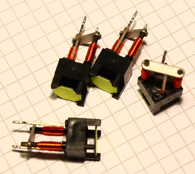
So one way to get an electromagnet is to disassemble a relay. Here's the core from a 12V relay, with the coil and the magnetic part to "loop back" and focus the magnetic field.
![]()
The electromagnet attracts the steel when energised - even a few volts, but the action is not "hammer-like" because one of the parts (the tube or the electromagnet) must move, and they are heavy, and this dissipates the energy, and the tube doesn't "ring".
Then there is the problem of remanence. Even after the pulse into the coil has ended, the electromagnet still sticks to the bar. Well, a freewheel diode across the coil seems to solve the problem.
I'd like the pulse to last for about 1/10s so let's see how much capacitance is needed : t=R×C, with R=57 ohms (approx). C=t/R=1500µF
I tried with 10000µF and it was apparently too much, but 470µF works well. You can vary the energy into the coil by changing the input voltage. And I have not even considered the inductance of the coil, which certainly messes with my estimates. I just checked : 68mH is not insignificant :-D
There is an obvious problem with the mechanical structure as the wire is a bit plastic and changes shape after several moves. Steel wire becomes necessary. The tube's fixation system is also not adapted for repeatability...
It's funny the things you find on youtube :-D
These guys made me consider using a non-magnetic hammer to prevent the sticking:
however my relay coil has no empty core to pass a hammer : I'll have to find something else. Even wind my own coil ?
And these little guys seem to have found a method for horizontal chiming but I wonder about the resonance mode:
If the tube is pierced, it may alter the resonance and the position does not seem to be calculated.
-
The Program Counter's circuit
04/08/2017 at 00:56 • 0 commentswork in progress, see also The instruction register (cont'd)
.
I've been focused on the main datapath but the control logic needs some love...
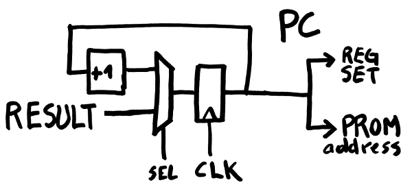
So let's talk about the PC, or Program Counter register.
From the user's point of view, PC is a user accessible register, that can be read as operand (only as the SRCX operand) and written as a destination. The value is incremented at every cycle to point to the next instruction so the value is visible both to the datapath and the PROM circuit.
From the hardware point of view : the PC is a register with a MUX2 (to select data coming from the datapath's result bus) and an incrementer.
![]()
How to use it and why
- Write an instruction address to PC so the next executed instruction is at the new address, as an equivalent of "BRANCH" or "JUMP" (it can be conditional)
- Read PC to perform operation on the current address and JUMP to a relative address
- Read PC to save it somewhere, just before you jump to a subroutine, to perform a CALL.
The last part requires a few MUX so the PC (actually, that's PC+1 so it returns to the next instruction) can be saved while the new address is computed.
![]()
To select the CALL path, we need a bit or signal in the topmost bits of the instruction (to save the other buts and keep the whole architecture orthogonal). That's hard because all the combinations and fields have been used. Except one !
The "NEVER" condition is now renamed "CALL" and behaves as "ALWAYS" but enables the necessary MUX.
Concerning the width : since the PC interacts with the datapath (more than I had considered initially) it becomes part of the bitplane. So 16+2 bitslices will be implemented. The backplane will enable and route the proper circuits.
In practice, not all bits might be used. The PROM can reasonably (at most ?) contain 1K instructions (that's up to 24K diodes guys !) and the address decoder really gets large at this point...
The PC's MSB (topmost bits) could be used to store a few bits at your own risks, because I'd love to create a SRAM-based PROM emulator (controlled by a Pi, serving YGWM, yada, yada...) and I can easily use the whole 64K addressing space :-)
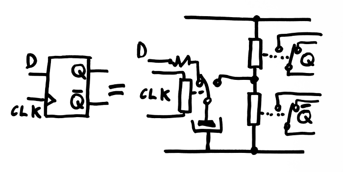
The PC's bits are implemented in CCPBRL, with a complementary output. Here is the equivalent circuit for a DFF : 3 relays and a capacitor are required, an additional resistor (in the 10-50 Ohms range) is added to reduce inrush current (and also protect from fast changing data if the input needs time to settle).
![]()
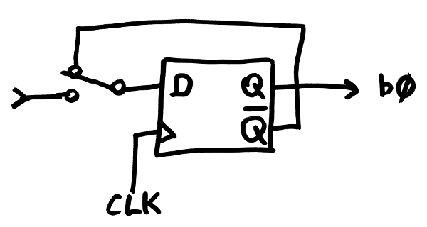
The LSB (or bit#0) is pretty simple : at each clock cycle, it toggles. So the inverted output is looped back to the input (through the MUX). Simple !![]()
(actually, that's a simplification because the carry in will always be set to 1 and every bitplane will use the same circuit)
For the other bits, it's barely more complicated : a MUX2 selects between Q and /Q, depending on the "carry in" signal". The real trick however is to get this carry signal...
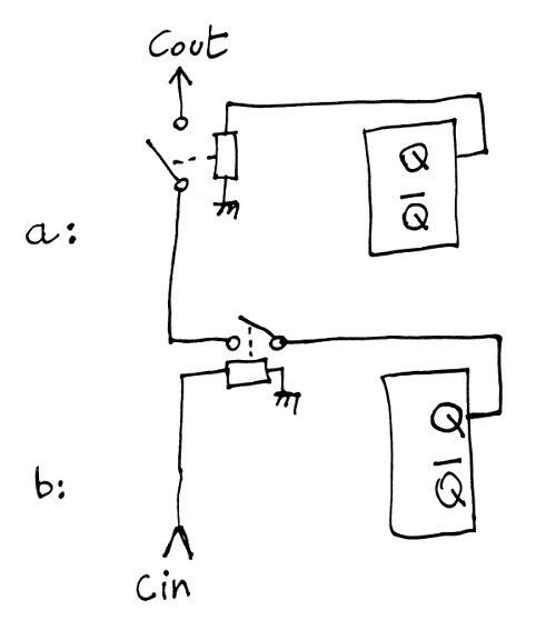
I know the usual method : the carry chain gets interrupted by a switch if the current stage is "1". That's method a) below :
![]()
But this amounts to a AND gate, right ?
And a AND gate can have its inputs swapped, right ? So look at version b) for which the signal passes through the coil.
The great thing about this is that the fanout is 2, which is naturally implemented with a CCPBRL cell. A (hypothetical) single incrementer stage is shown below:
![]()
OK it slows the signal down... However, it's possible to
- alternate between circuit a) and circuit b) to halve the propagation delay
- include the carry chain switch's coil inside the DFF circuitry, but that requires 6V power and corresponding signals, to swing between 6V and 12V, and a resistor will waste energy
The incrementer should be quite fast because we want PC+1 at the same time the ALU delivers its result (so it can be written to the register and/or the memory).
The typical carry interrupted AND chain has a big problem with variable load (driving 16 relays can draw a lot of energy and damage the relays' contacts. But the PC+1 should be available in about 5 coil units (time to decode the instruction address, read/decode/amplifiy the control signals ...)
-
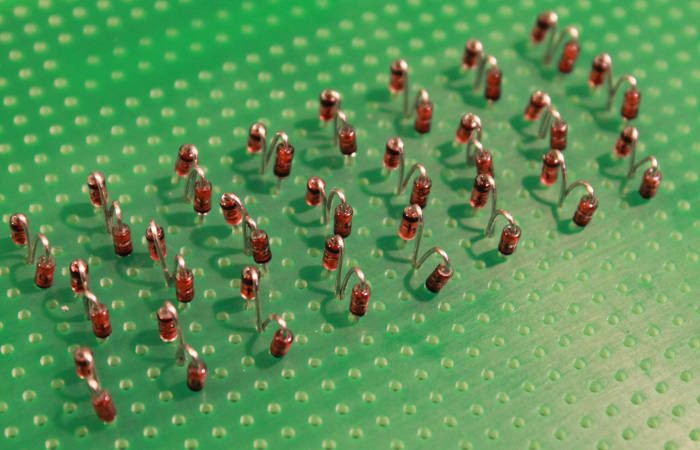
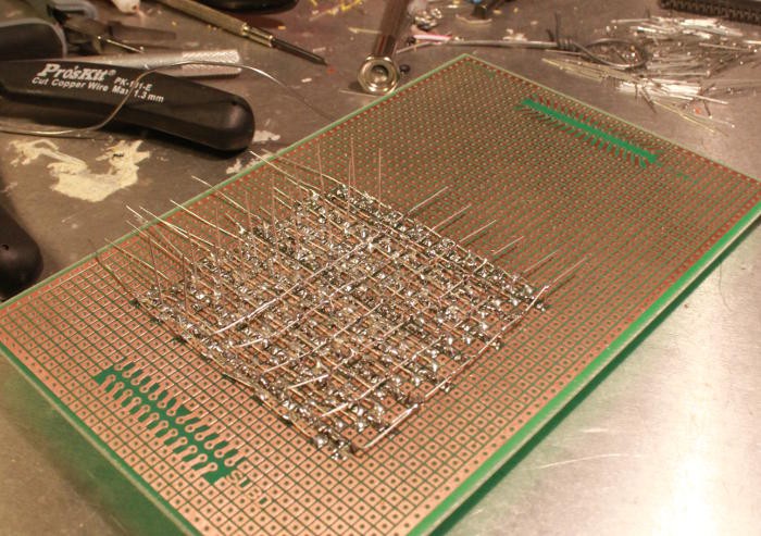
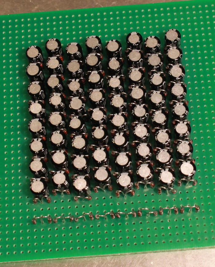
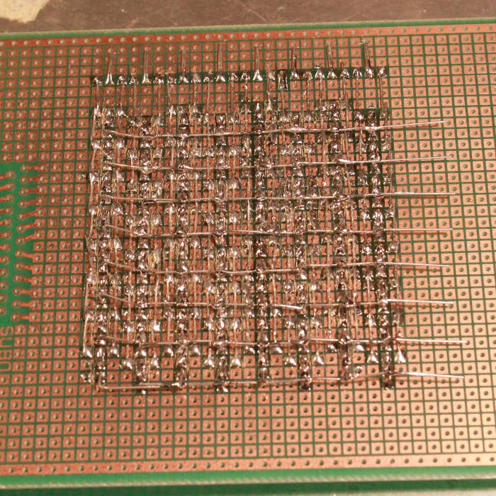
First DRAM array prototype
04/07/2017 at 06:03 • 20 commentsFollowing the recent updates about the DRAM (in the log DRAM (again)), I had to test all my assertions and try with the real parts.
The BAS70 are apparently not practical for a prototype because I have no suitable PCB. I'd have to put a lot of wires... But I found a method with the legs of two 1N4148 !
It was a pretty crazy adventure but it ends well (so far, if you don't count the 30 capacitors I soldered in reverse).
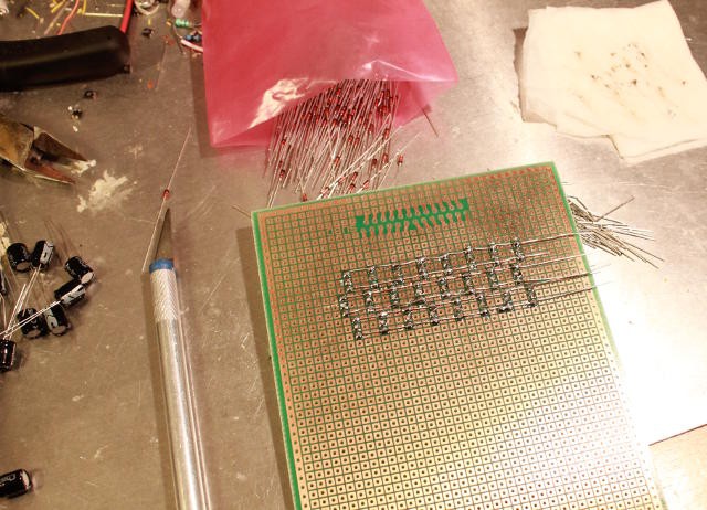
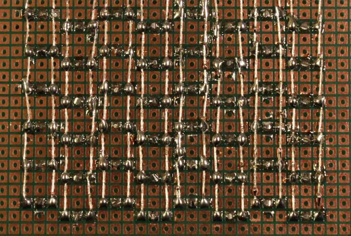
I figured out a placement that is feasible and compact, but it requires two levels of wiring. First, the diodes are soldered in place and their wires occupy the PCB surface :
![]()
![]()
Make sure they are ALL in the correct direction :-) before it's too late...
![]()
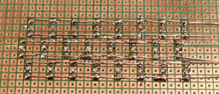
I have chosen to alternate the positions to prevent soldering problems :
![]()
of course, it's still important to test ;-)
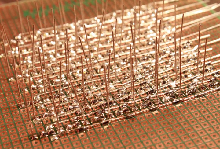
Then the capacitors. Make sure they are properly oriented ! (I wasted 30 of them...)
![]()
The positive side is connected to the diodes with a solder bridge and the other stands alone, waiting to be bent.
.
Side view :![]()
![]()
The finished board :
You can see the "re-steering" diodes at the bottom. That's where data bits will go :-)![]()
It's a pretty big mess of wires ;-)![]()
Tomorrow I'll wire some switches...
-
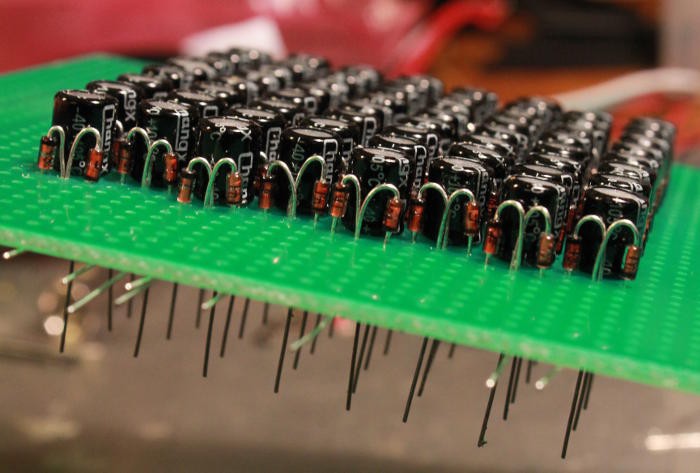
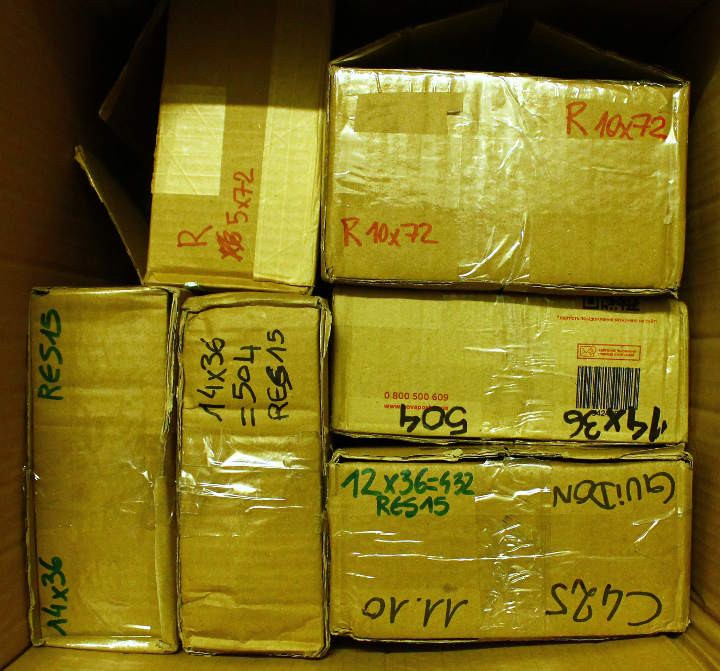
I hope that's enough
04/06/2017 at 09:29 • 0 commentsSo I've been updating the inventory and here are the relays :
![]()
That's approximately 3000 relays, so I'm good.
I also have 10 capacitors (100µF 25V) but the sizes are mixed (4K in 6×7mm and 6K in 5×11mm). This does not help making a compact DRAM board, I'd like to fit 16×16 in a 10cm square... 16×5mm=8cm so I have room for connectors on 3 sides.