 Matt Lacey
So the 68k CPUs use an asychronous bus setup such that when the CPU asks something else for some data (e.g. RAM) then rather than just assuming the data will be there in a given amount of time, it sits and waits until it's told the data is ready and present on the bus. This signal is called DTACK (Data Transfer ACKnowledge), and you pull it LOW to tell the CPU it's good to go.
For the initial freerunning stage (the part I logged before getting sidetracked by EEPROM programming) this can just be grounded, and if you have fast memory, it could just stay that way. For now I'm implementing a pretty dumb scheme that's in no way optimal, Rather than considering all of the CPU signals that can indicate an address is valid and ready I'm just taking the easiest option.
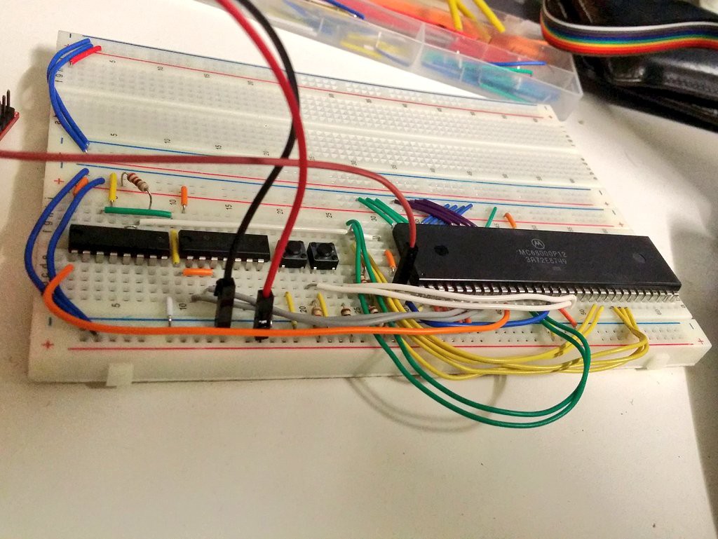
The 68k has two control lines called the Upper Address Strobe and Lower Address Strobe, and if either of these are asserted LOW then it's attempting to perform a read/write. Right now I'm taking those two lines, running them through a 7408 AND gate, and pumping the result through another SN74HC595N shift register (the same type I used in the EEPROM programmer) to delay the LOW pulse before passing it back to the CPU on the DTACK pin. Dumb, not optimal, but working. That'll do for now: I know from programming that premature optimisation will bite you in the ass eleven times out of ten, and so far my adventures into hardware have been fraught with more than a few dumb mistakes, so consider this an attempt to mitigate my own stupidity.
Discussions
Become a Hackaday.io Member
Create an account to leave a comment. Already have an account? Log In.