 Tom Anderson
Enter constraints, derive component values, choose components, draw schematic, draw layout. Welcome to analog land!
The constraints are in Excel. To really check to make sure that everything will work, I can use a simulator. More time in the simulator increases the odds of first-pass success.
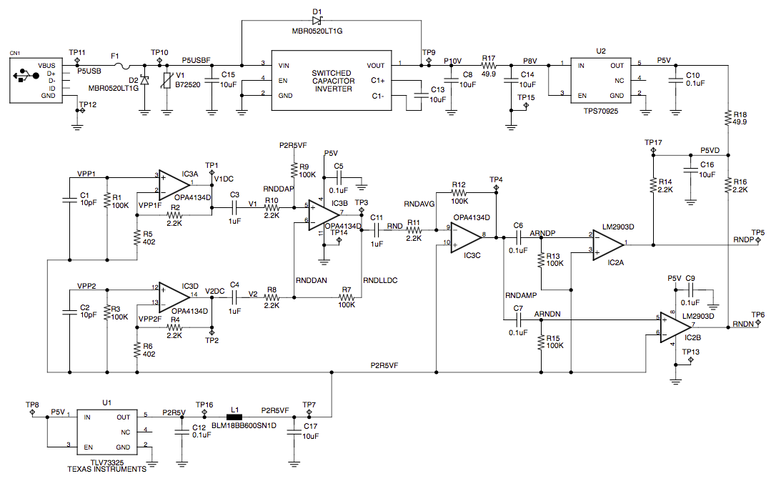
The challenge with this design is to make a random noise source where the noise comes from a well-known, testable source. Other components are not allowed to make a significant contribution to the noise. The intended noise source is a pair of 100k resistors. I think of the thermal noise from these resistors as the 'signal', which I need to process in a low-noise way. This is similar to a sensor project, in that I need to take a low-level signal and amplify it to a useful level. Since thermal noise is a low-voltage phenomena, the signal level from it is low. How low? Noise is interesting that way - the more bandwidth there is to measure it, the more noise there will be. Today's version of the design has 13.3kHz of bandwidth, and for two 100k resistors, the noise level comes out to 20.8uV RMS.
I call the resistors being measured the 'physics package' and the noise coming from them the 'signal'. The noise from the circuit that is not from the resistors is still called 'noise'.
To get low noise, I am using the OPA4134 opamp. The resistors are thin-film 0.1% 25ppm/degC. The design technique is the same that I use for designing test equipment. The board will be four layers, with a solid ground plane and a split ground/2.5V plane, and two routing layers. This, and far more power filtering than you might think would be strictly necessary, are important for building accurate circuits with low-level signals.
The network with L1 and C17 is designed using the technique from my blog post "Power Supply Filter Design for Printed Circuit Boards". The damping comes from the series resistance in the bead L1. When I run a simulation of the board, I should be able to post performance results for the power supply bypassing as well as the noise.
This is my first EAGLE schematic and there is still some cleanup to do. I also need to run a simulation, but I haven't chosen my approach for how to do that. In making the EAGLE schematic, I made a local library in the design that has the parts that I am using. I created the library by cutting, pasting, and editing the XML library file in Sublime Text. For me, this is easier than a GUI. Understanding the data format is the main way that I learn CAD tools. In my mental model, a GUI is a tool that makes it easier to create a design database. If I can't easily see the design database, the tool is much harder to learn. EAGLE is delightful this way! The symbol, schematic, and layout files are human readable.
This schematic is good enough for a first-pass at layout. There are plenty of library problems that I see in layout, and I don't quite have the UI tamed yet, so it looks like this:

My plan is to rip up the routing, adjust the placement, and route again. There is a 'long pole' starting at the resistor R5 sticking out the bottom row. This is not so hard to fix, and I need to move V1 and D1 close to the top anyway. There is plenty of free space. I am using wide traces to make the board easy to modify without damage. When traces are too wide, they are hard to cut. When they are too narrow, they become too fragile. The optimum width for rework is in the .012" to .025" range. Wider traces in this range are easier solder wires to. There are big test points on all the important nodes, except where there are space issues. There are a lot of test points on ground! Space around the edge of the board, and plenty of mounting holes make it much more fun when it is time to work on the board.
The resistor noise sources are R1 and R3. The layout is symmetrical for these two parts, which creates a string of devices starting with R5. There is a traffic jam around C15. There is plenty of room to solve these problems, but taking advantage of it means that the existing routing has to go! This is no problem, though. I am getting better at manual routing anyway.
Discussions
Become a Hackaday.io Member
Create an account to leave a comment. Already have an account? Log In.