 novirium
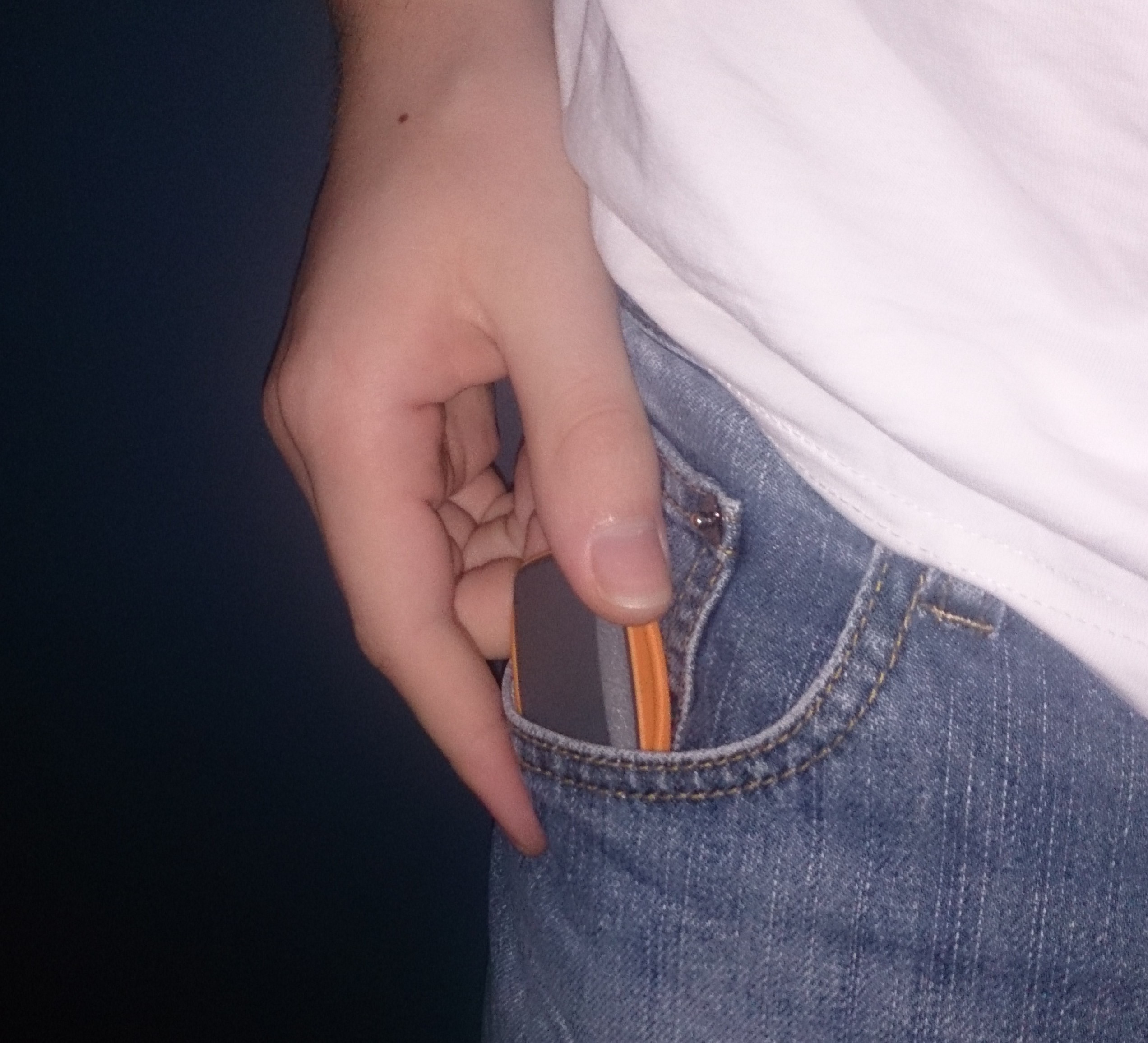
I will admit to committing a cardinal sin of electronic device design - I picked the enclosure before designing what needed to go in it. This is one of the reasons I'm designing another hardware iteration, and had a few implications that can be seen in the current device - there is way too much empty space, the battery is being just slightly compressed, and the USB port is sticking out the large, flat side of enclosure, rather than the edge.
Enclosure
The enclosure used is part of the OKW Minitec range. They're pretty diverse enclosures, and you can order the different parts in lots of sizes and colours to mix and match. This one appealed to me simply because I wanted to try and cram the device into something small, and it was curved and comfortable to hold while still offering mounting points for a strap. It comes apart into three pieces, with the center ring being made of a flexible rubber.
To make room for the USB port, a hole was drilled in the front face, along with two smaller holes in the underside to let air flow through to the humidity sensor.
PCB
Having a curved enclosure might be great for aesthetics, but it really does make the PCB design a bit of a pain. Unable to find a way to generate a cross-section at the point where the PCB meets the enclosure edge, I actually resorted to manually cutting the CAD model and reading off vertex coordinates, translating them to line dimensions in KiCad. It took...a while, and I wouldn't recommend anyone else doing it that way, though it does seat quite neatly on the curved inner surface. I'm pretty sure the newer version of KiCad can now import DXFs anyway.
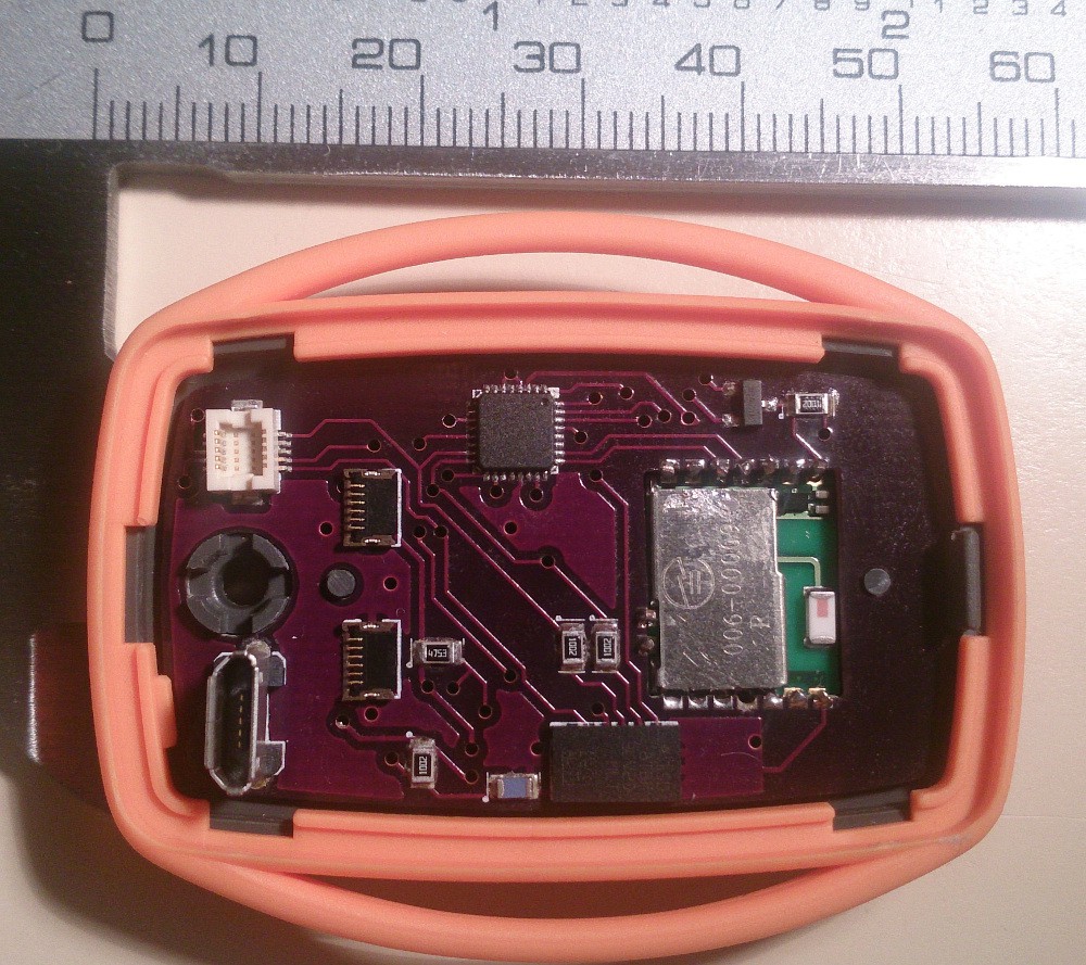
The general PCB layout was dictated by the larger components that really only had one place to go. The Bluetooth module can be see down one end, inset into a cutout. Not only did this make it easier to solder to the edge castellations that the module uses, but it was the only way to keep the board thin enough to fit under the battery. Note that the end around the chip antenna is essentially empty of components and pours - the Bluetooth datasheet was pretty specific about this, and it makes sense to keep interference away.
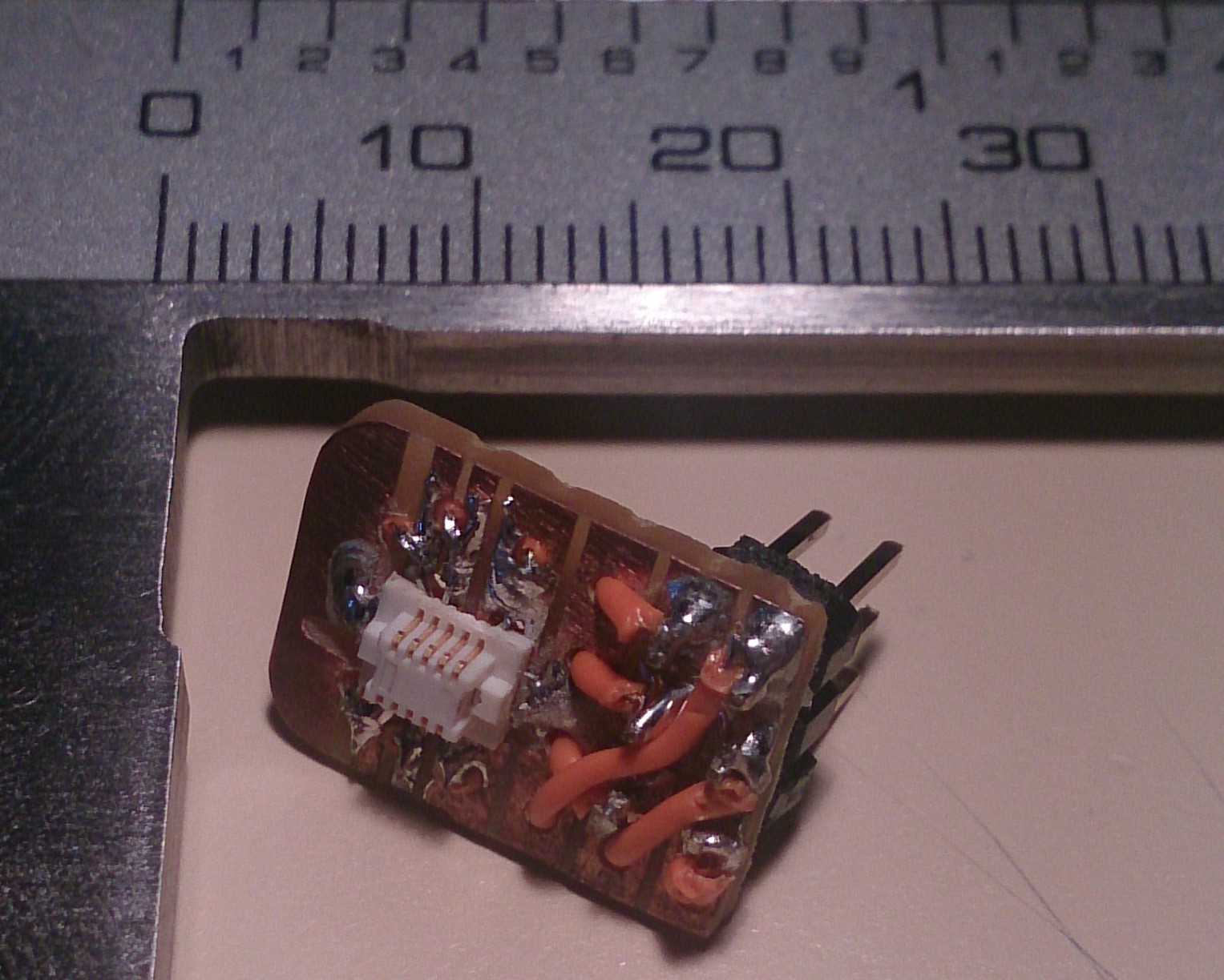
Up the other end is the USB and programming connectors. Both were too tall to fit underneath the battery that lays over the board. Finding a connector that would fit inside the enclosure but still allow a vertical connection for programming was difficult, and I eventually the DF12 series of surface mount stacking connectors. The pitch on these things is tiny, and it wasn't until construction that I actually thought it through and realised an adapter to the standard 6 pin ISP would be needed. Turns out you can do some pretty tiny stuff with strip board and a craft knife.
To the right of the USB connector are the battery terminals. The intention here was to get something that could clamp onto the thin tags used on flat LiPo batteries, and I bought some FPC connectors to try - using all pins on each connector to clamp onto the tag. This actually worked pretty well, other than the difficulty of closing the connector down once the battery is on top of it (requires very fine tweezers).
Everything else was pretty much standard layout procedure - the power supply and humidity sensor are on the reverse side, to spread around the board realestate a little. That said, I've learnt a lot since making these boards, and so won't be surprised if people find things that could work better. I'm always happy to learn though, so let me know in the comments.
Discussions
Become a Hackaday.io Member
Create an account to leave a comment. Already have an account? Log In.