So we’ve talked about how to keep track of where we are in a program, but we haven’t talked about how we actually decide which parts of memory are actual opcodes, which are operands, and which are just data. That’s a pretty involved process, so we’ll split it into 2 parts and here we’ll talk about the basics of how instructions are executed and how they get loaded into the CPU (we’ll save the actual interpretation of those instructions for later). To start, here’s the block diagram for loading instructions:
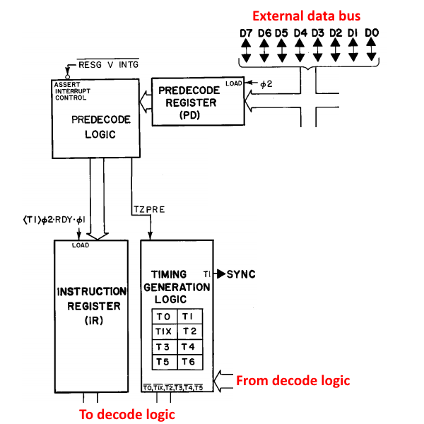
Starting from the top, we’ve got the external data bus which shuttles data between the CPU and memory (it’s a tri-state bus that can both read and write, but we’ll ignore the writing part for now – so for this post, it’s just a data input bus). Next, we have the pre-decode register, which gets loaded with the contents of the data bus on every phase 2 clock. Note that that’s every phase 2, so it’ll get loaded with junk a majority of time and we have to figure out when it’s not junk. Next we’ve got some pre-decode logic, whose main function is to replace the pre-decode register data with a pre-determined opcode during an interrupt. We’ll get to interrupts later, so just remember this part and, for now, ignore it. Finally, we have the brains of the thing: the instruction register and the timing logic.
First, some basics: every instruction takes some number of CPU cycles to complete (remember that 1 cycle is made up of a phase 1 and phase 2 clock). To determine what happens on every cycle of the current instruction, the instruction decode logic must take into account both the current opcode and the current cycle. However, the number of cycles per instruction varies, and isn’t necessarily fixed even for a single instruction (things like branches take a variable amount of cycles, for example, and even accessing memory in certain locations can add cycles as we’ll see later). So the decode logic also needs to control the timing logic in order to keep everything synced up, and we get a big feedback loop.
Now with that basic idea, we can get down to how it actually works. There are 8 cycles the CPU can be in (in the block diagram, there’s a T1X cycle for some reason, but my implementation just goes from 0 to 7 like a normal person). The longest instructions only take 7 cycles to complete, but there are 8 labels since a few instructions can skip a cycle (to be explained later). Anyway, every instruction is set up to fetch the next opcode during the 0th cycle. So during the 0th cycle, the CPU will send out the address of the next opcode during phase 1, then the fetched data is latched into the pre-decode register on phase 2. Then, that data is finally latched into the instruction register on the following phase 1 (of the 1st cycle). This all works because each instruction knows when it's done and should fetch the next opcode, and if it was implemented correctly, the program counter will be pointing at the next opcode.
Ok, well, that was a lot of background for a pretty straightforward thing, so here’s the code!
module InstructionController(
    input sys_clock, rst,	     // Main system clock and reset
    input clk_ph1,		     // clock phase 1
    input [7:0] PD,		     // pre-decode register
    input I_cycle, R_cycle, S_cycle, // increment/reset/skip cycle counter lines
    input int_flag,                  // perform interrupt
    output reg [7:0] IR,             // instruction register
    output reg [2:0] cycle,          // current instruction cycle
    output [2:0] next_cycle          // next instruction cycle
    );

// Signal declarations:
wire [7:0] opcode;      // Opcode to put into instruction register

// Decide what the next cycle count should be:
assign next_cycle = (R_cycle == 1) ? 3'd0                                             // if reset_cycle, reset count to 0
                                   : (I_cycle == 1) ? cycle + 3'd1                    // else, if increment_cycle, increment count
                                                    : (S_cycle == 1) ? cycle + 3'd2   // else, if skip_cycle, increment count twice
                                                                     : cycle;         // else, don't change count

// Decide what gets loaded into the instruction register (change only on T1 cycle):
assign opcode = (next_cycle == 1) ? (int_flag ? 8'd0 : PD)  // on next T1, load new opcode or BRK (0) if doing an interrupt
                                  : IR;                     // if not T1 cycle, keep last opcode

// Latch new values on ph1:
always @(posedge sys_clock) begin

	if (rst == 0) begin
	    cycle <= 0;		    // Reset cycle counter to 0
	    IR <= 0;		    // Reset IR - starts out in BRK to start reset routine
	end
	else if (clk_ph1) begin
	    cycle <= next_cycle;    // Latch cycle
            IR <= opcode;           // Latch opcode
	end

end

endmodule
Ok, we’ve got the system clock, reset, and the phase 1 clock as inputs. We’ve also got three control signals that are generated by the instruction decoder – these control the cycle counter. Other inputs are the pre-decode register (PD) and an interrupt flag (if an interrupt was previously detected, we need to start the interrupt service routine). Then the module will output the current instruction in the instruction register, the current cycle, and the next cycle which will happen (the interrupt controller needs this information because of its awkward timing).
The first thing the module does is compute what the next cycle should be based on the input from the decoder. The cycle can be reset to 0, incremented, or incremented by 2 to skip a cycle. One of these should be done every cycle, but we’ll throw a default of staying the same to make sure. Then, we’ll figure out what to load into the instruction register on the next phase 1. We only load a new value on cycle 1, otherwise keep it the same. On cycle 1, we’ll load in the pre-decode register (which was filled on the previous phase 2) if there’s no interrupt going on. The interrupt will take precedent though, and will load in 0 (the “BRK” instruction). Then, we’ll latch the new values for cycle and IR on the next phase 1.
Aaaaand, that’s pretty much it! Next we’ll get into more of the decoding, which should be exciting (or maybe we’ll go through more of the CPU infrastructure… hmmm, TBD).
Discussions
Become a Hackaday.io Member
Create an account to leave a comment. Already have an account? Log In.