Ok, first post! So far, I’ve implemented the CPU and absolutely nothing else, so here we’ll go through a super quick overview of the NES CPU and then get into details of the code in further log posts. The CPU has been previously documented way more thoroughly than I could ever do (see, for example, the good folks over at http://wiki.nesdev.com/w/index.php/NES_reference_guide), so we’ll keep this brief.
The NES CPU (the Ricoh 2A03) used a variant of the 8-bit MOS 6502 processor as its core (the 2A03 contains the 6502 core along with some I/O registers and an audio processor). The only difference in the Ricoh 6502 and the original MOS 6502 is that the former lacks the decimal mode found in the original, so the real work here is implementing the 6502.
The main references I used were Donald Hanson’s block diagram of the 6502 and the MOS programming and hardware manuals (see the “Docs” folder on the GitHub repo). Well, those along with the literally thousands of pages of information on the NesDev wiki/forum and elsewhere on the web (also, a shoutout to another NES FPGA implementation from Brian Bennett, which helped me out more than a few times when I was stumped - https://github.com/brianbennett/fpga_nes). I’m going to throw the 6502 block diagram in here for reference, since things make a lot more sense (to me, anyway) looking at it.
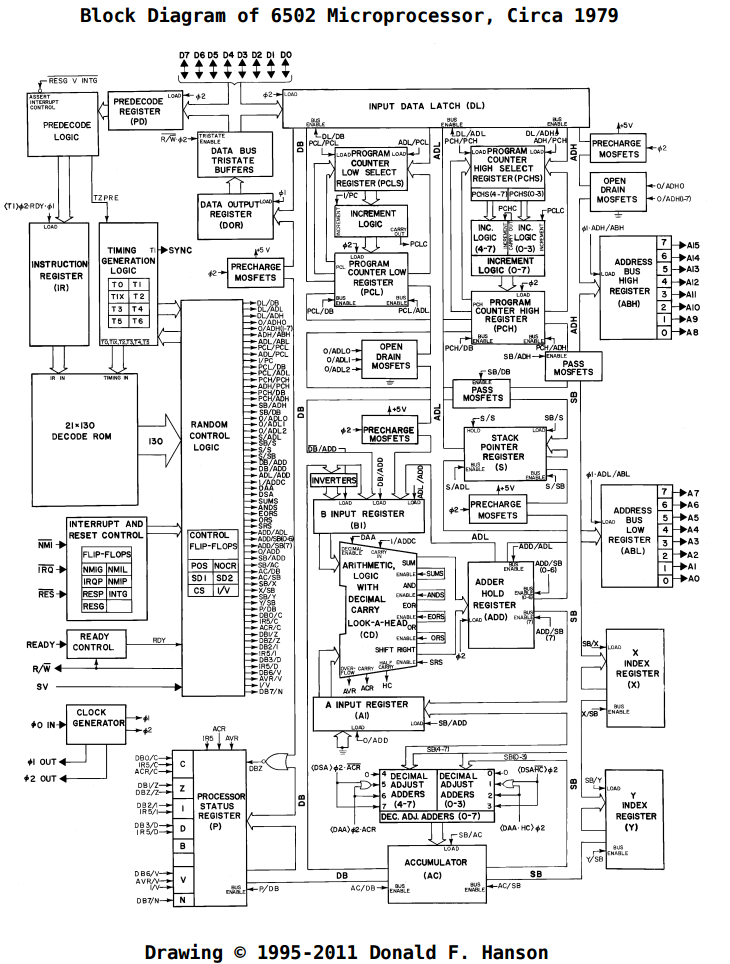 Some basics: The 6502 is an 8-bit processor, with a 16-bit address space. It has 6 internal registers (3 special purpose – the program counter, status register, and stack pointer – and 3 general purpose – X, Y, and the accumulator). The registers are linked to the various parts of the CPU through 2 main internal buses (the Data Bus and the Special Bus, DB and SB in the block diagram), along with 2 buses dedicated to shuttling the low and high bytes of the address around (ADL and ADH in the block diagram). There are also interconnects between buses so you can connect them together and get data wherever it’s needed. The ALU is pretty central in the design: besides the usual operations on external data, it’s also used for internal purposes like temporarily storing data and addresses while other data is being fetched as well as computing addresses for some of the more complicated addressing modes. All of this is coordinated and controlled via the opcode decoder, which decides what to do on each cycle of each opcode.
Ok, that probably explained exactly zero, but we’ll leave it there for now. In the next log, I’m going to start explaining the ALU and my implementation of it.
Discussions
Become a Hackaday.io Member
Create an account to leave a comment. Already have an account? Log In.