 Chris.deerleg
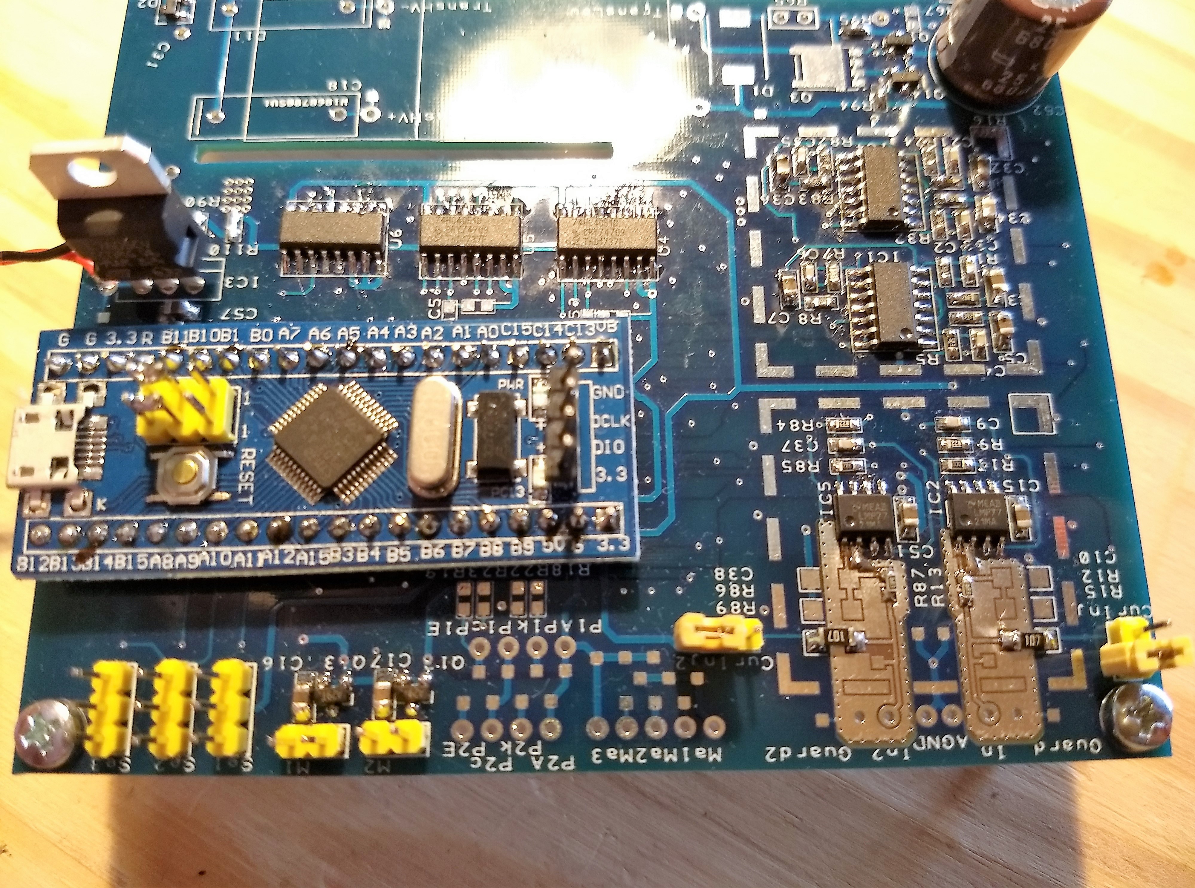
On the image above it the PCB shown which I made. I right lower corner of the PCB are the Femto ampere amplifier placed . The plain area surrounded with vias are the guard ring as I describe in the last log entry. On the guard ring is the solder mask removed to get the bare resistance of the FR4 base material and don't "short" the FR4 resistance by the solder mask . The square pattern around the Femto ampere amplifiers are for a EMI Gaskets to improve the shielding for the case that I run in to EMC issues. In the square pattern above the Femto ampere ampere amplifiers are placed the secondary amplification stage with the MAX4450.
Discussions
Become a Hackaday.io Member
Create an account to leave a comment. Already have an account? Log In.
This approach should work with high beam currents. But SE in SEM are usually detected by scintillator and photomultiplier. There is a grid with positive potential (~250V) which sucks the SE electrons, these signal SE are accelerated towards scintillator and converted to photons. Im building SEM too and my plan is to use one of these instead of PMT: https://www.hamamatsu.com/eu/en/product/category/3100/4004/4113/index.html
Are you sure? yes | no