 Jorj Bauer
See that MS6264 sitting by its lonesome on the left under the program counter? Well, it's 'bout to have something to do.
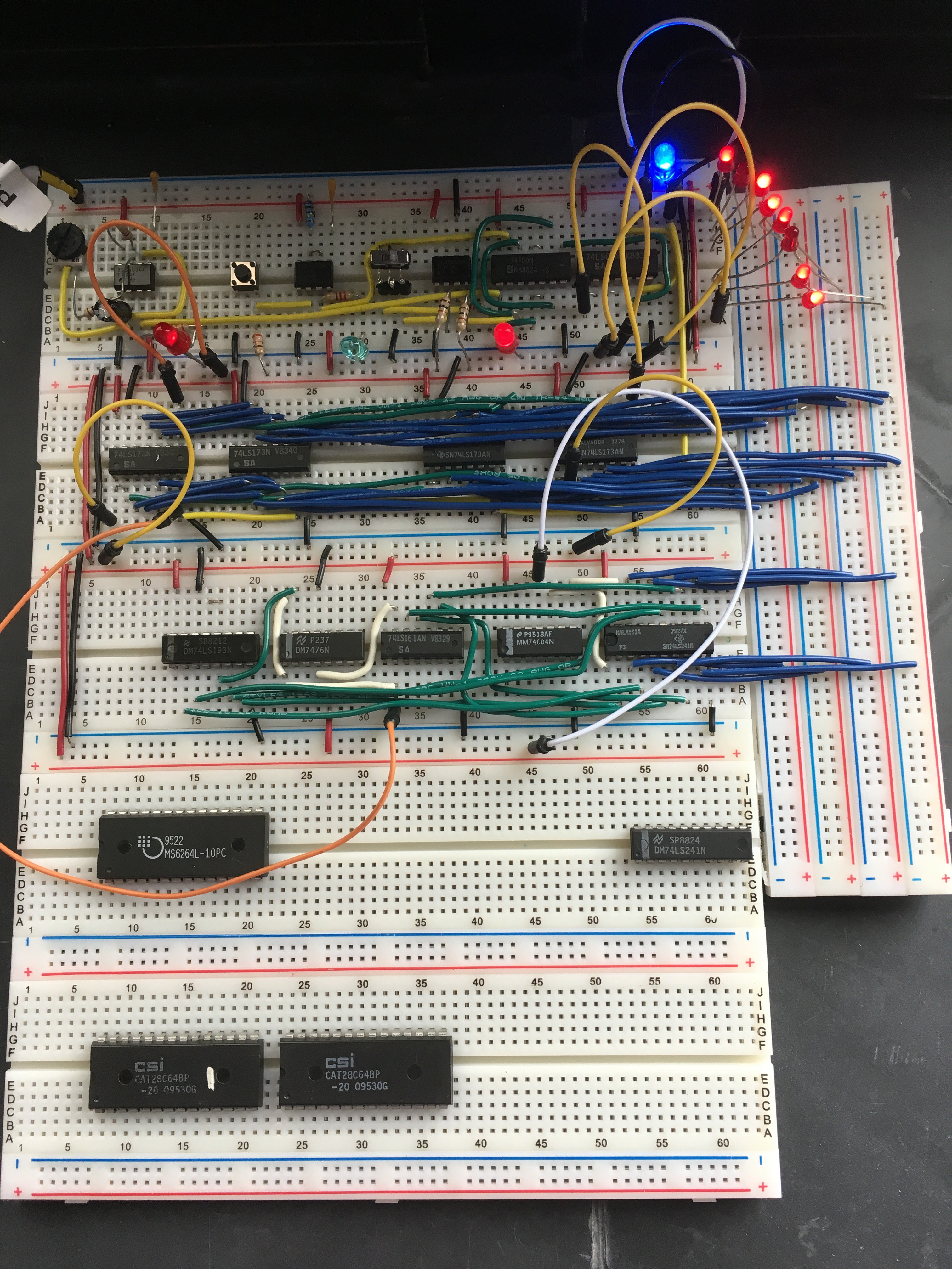
The MS6264 is a 64-kilobit static RAM. I found two of them in my stockpile (salvaged from old GatorBoxes, I think, along with the EEPROMs and a pile of 68000s). I would like to be able to address all 8k of it, one 256-byte page at a time - but let's start with just 8 bits of address space. That's one 256-byte "page" of memory.
I've only used one bus transceiver so far because I've only really needed to buffer the program counter output from the bus. Here, I'm going to need an input and output tri-state buffer, because I might be reading from the RAM (output *to* the bus) or writing to the RAM (input *from* the bus). This would be the perfect use of a '245 -- an 8-bit transceiver that has a simple direction setting bit. But I don't have those lying around. What I do have is two '241s; one '367; and one '244. Each of those is a 4-bit bidirectional switch (or an 8-bit unidirectional switch) so I'm going to need two. I guess the best way to deal with that is to reclaim the '241 that I just used for the program counter, replacing it with the '244; and then using the two '241s for the RAM.
The difference between the '244 and the '241 is minor. If you look at this datasheet for the 74x24x family of buffers, section 8.1 shows the differences -- on the '241, the 1G enable line is active-low while the 2G enable line is active-high. On the '244, they're both active-low. Which means that the 7404 hex inverter is no longer necessary for the PC counter output - bonus!
Staying with that 7404 inverter for a moment: instead of pulling it out, there's actually another use. The clear lines for the program counters on the two PC counter chips are also different logic senses. I'd like to have a power-on reset that explicitly holds them at "reset" while the power stabilizes - along with keeping the clock output halted - which means I still want that inverter there. Oh well.
Back to the RAM, then.
Two '241s, one 8k RAM chip with the high 5 bits tied to ground. The RAM I/O pins go to the '241s, which are wired as 4-bit bidirectional buffers. But where do the address lines come from? How do we select the address of RAM that we want to store or fetch?
I guess we're going to need another 8-bit register to store the current memory address. I have more of the '173s, so they'll do just fine. And they should also feed from the bus, so that we can set them...
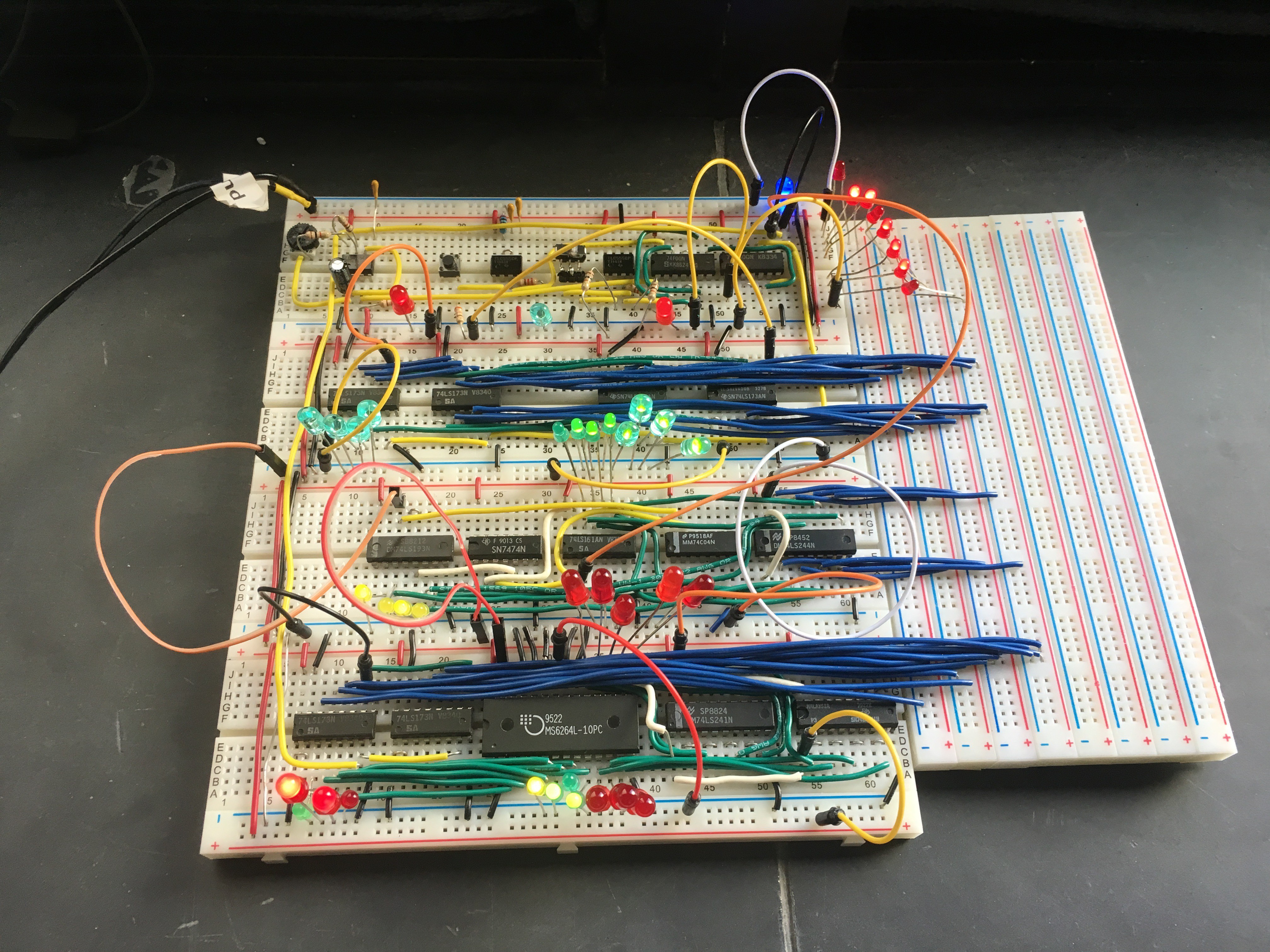
And *poof*, one RAM module wired up. There's an enable line to load the memory address register from the bus; an enable line to connect the RAM module to the bus; and a RAM write enable that's tied directly to the enable that inputs RAM from the bus. It's a heck of a lot of wire in a small space, but it works...
Discussions
Become a Hackaday.io Member
Create an account to leave a comment. Already have an account? Log In.