The first revision of the IuT voltmeter was built using the Wemos mini prototyping system, in particular D1 mini board and matching shields: dual base, battery shield, protoboard shield.
(Note 1: more about Wemos D1 mini shields - at the end of the log entry)
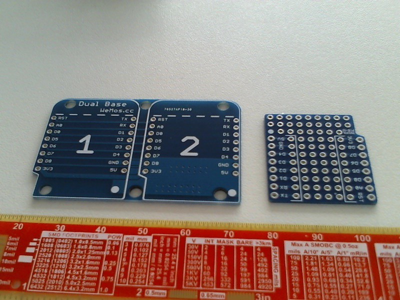
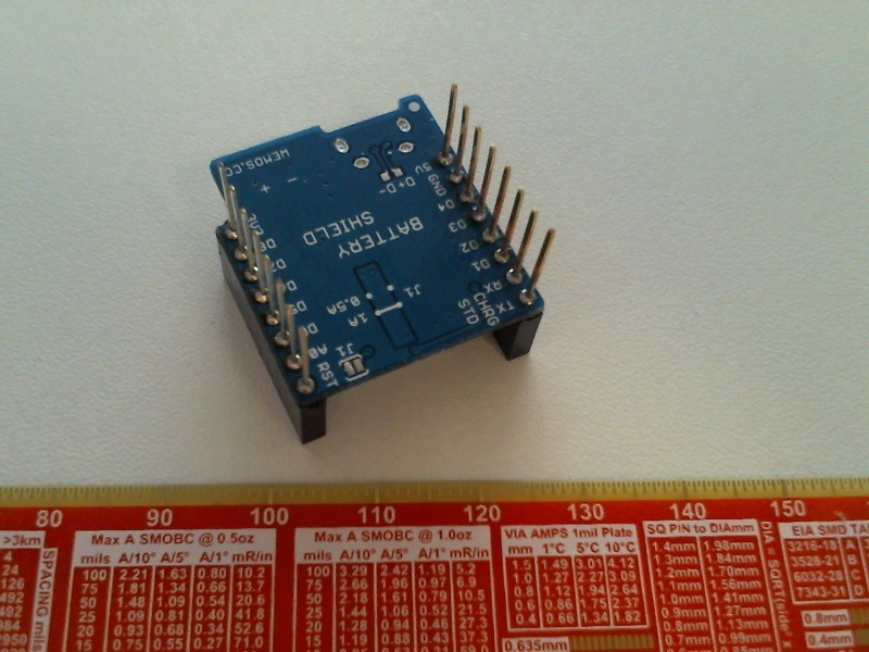
Dual base and protoboard shields are shown in the picture below with a ruler for scale:
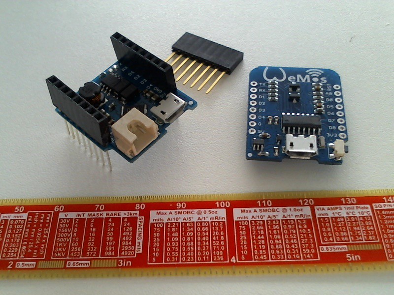
 The battery shield is on the left, the header with protruding pins to stack the boards in the centre, and the D1 mini board on the right.
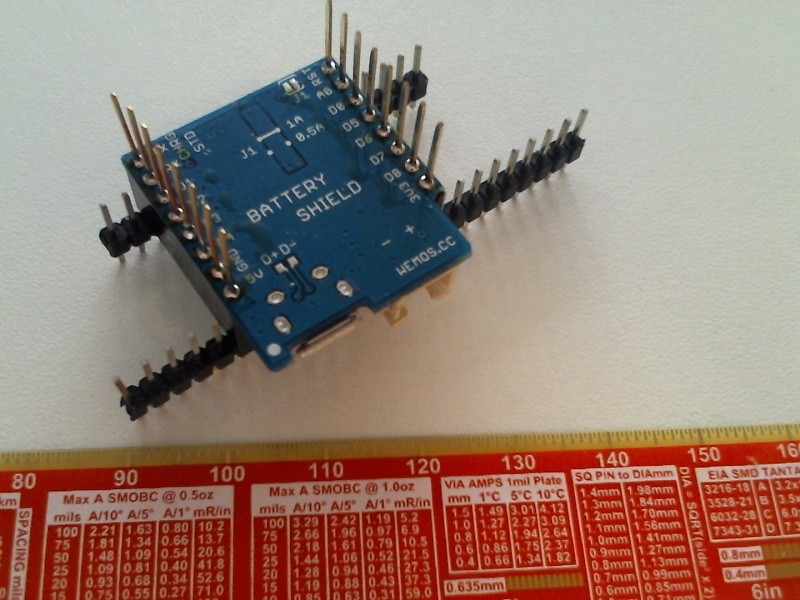
 Some care is required when soldering the stakable headers to keep them aligned. I used a spare male pin header as shown below:
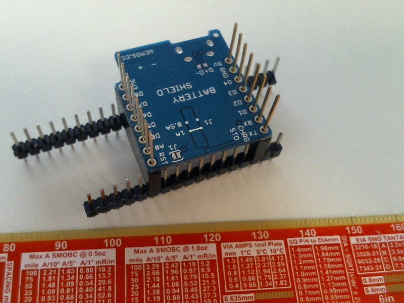
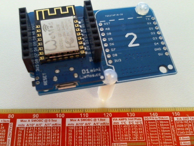
Every Wemos board has a cut out. In order not to short shields one should use the same direction for the headers on all the boards. I placed the cut out as shown above in order to have the soldered SMD components between the female pins.
I always use extra flux for soldering (Note 2: why use some extra flux and what are the options). Flux left some residue
 which was removed later:
I wanted to save some space with this prototype and have flexibility to adding more shields. For this reason I soldered the D1 mini board and battery shield to the base directly (rather than using extra female headers on the base) and used spacers to support the base. Here is the view from the bottom
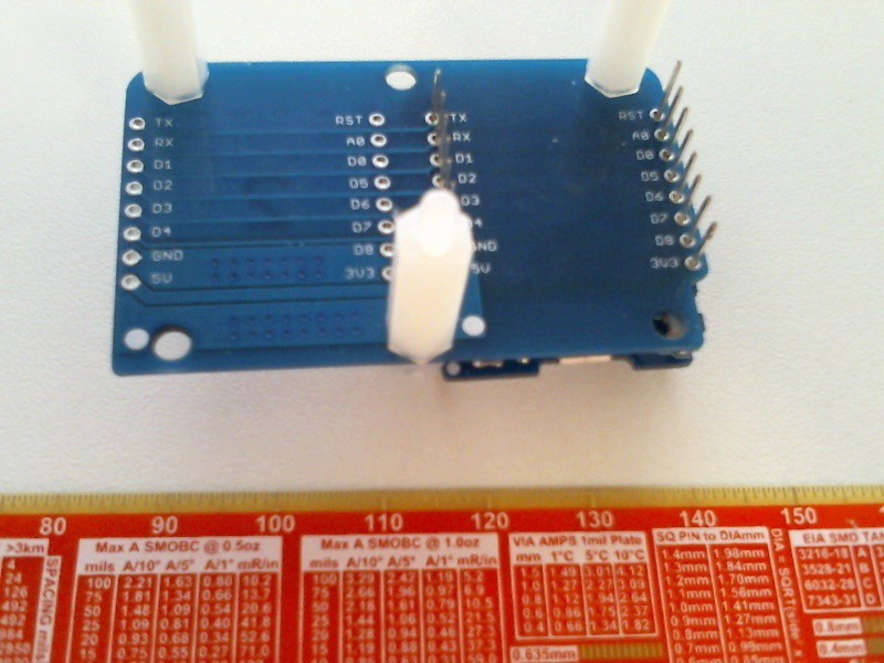
and one from the above
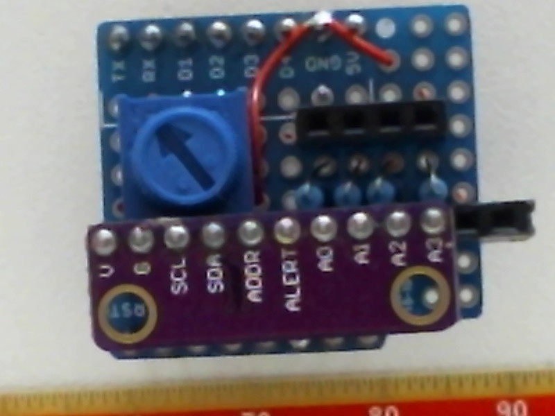
The protoboard shield was used to attach a female header for a standard ADS1115 (or ADS1015) ADC module (Note 3 : the differences between ADS1115 and ADS1015 ADC modules). I mounted D1 mini common header pins (both sides of the protoboard), a female measurement socket for connecting male-to-male wires to the breadboard (left of the centre); female socket for the ADC module (right of the centre), four resistors connected in series between the module's inputs and the measurement socket for input protection discussed later (leads visible between the female sockets),
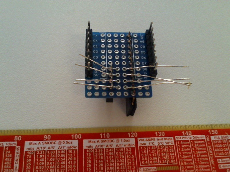
and connected interface pins of the ADC module to the D1 mini pins.
The module uses I2C nterface which requires connecting respective SDA and SCL lines of the D1 mini and module together (no note here as there are plenty of resources on the net, I only briefly menton a few essential things). The module integrates compulsory pull up resisotrs for both the lines (10k each). Wemos I2C shields use pin D1 as SCL and D2 as SDA; this convention was followed here.
By onnecting the ADR pin differently, the user can select one out of four available I2C addresses. I connected the ADDR pin to GND selecting address 0x48.
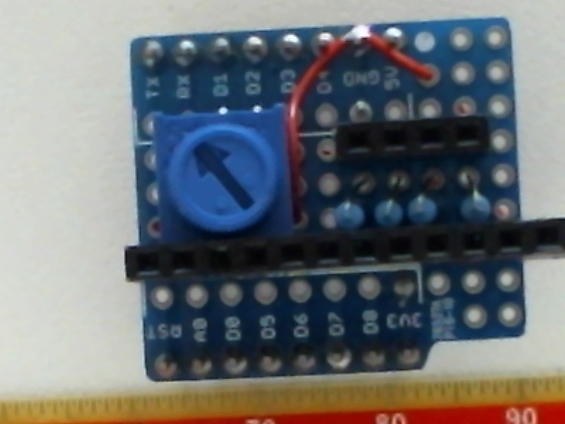
As the board still had some unoccupied space, I added a potentiometer
(pot) to enable the board's self-contained testing by connecting an ADC
channel to the pot's wiper. The oher terminals of the pot were wired to
the ADC module's power supply rails.
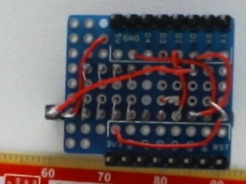
The complete connections diagramm is shown below

That is how the shield with the ADC module looks from the top
 The same shield with the ADC module removed shown from the top
and from the bottom
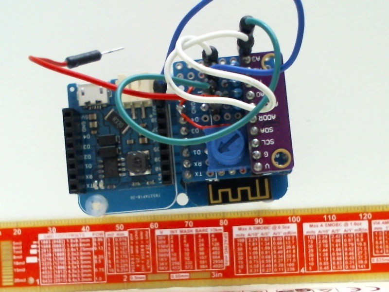
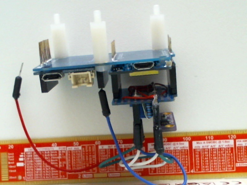
When the assembly was first plugged into a PC USB port, the LED on the D1 mini board momentarily blinked indicating correct operation. At this stage I considered construction of the revision 1 completed. The photographs below show how the final assembly looks like with the jumper wires connected to various pins (3.3 V, ground, potentiometer) for testing purposes.
Note 1: more about Wemos D1 mini shields
Originaly D1 mini modules and shields were supposed to be connected like Arduino Uno and its stackable shields. However some of the shields are too tall (e.g., relay shield) and need to be placed on the top of the stack to be useful (e.g., button and OLED shields). Dual base shield addressed this shortcoming, and 'tripler base' shield was introduced recently.
Dave Jones from EEVblog recently used a Wemos mini module and discussed his experience of programming it with the Arduino IDE.
Note 2: why using some extra flux and what are the options
Soldering uses molten solder to first wet metal pieces then to hold these together when the solder solidifies. The surface of these metal pieces is commonly covered with oxides and other substances/films that prevent the solder from wetting them properly. Flux dissolves these contaminants then evaporates with visible smoke.
(In the past people used to inhale these smokes and it did not make huge impact on their life expectancy because they suffered much more from oter things. However if you want to claim your pension for some time after getting retired, get a proper fume extractor or at least have some fan to blow the fumes away from you.)
Most people use either 'no clean' or 'water soluble' flux that do what their names say.
'Water soluble' flux is preferable if you want to demonstrate your board for some academic or social credit; it is used in industry for some consumer products. To remove the flux residue, use warm water with some soap/detergent/washing up liquid and lint-free brush. Watch out for
1) removing the residue quickly enough; if left for substantial time (say, a few days), this flux might corrode the board and components;
2) there are components that do not like to be bathed like speakers, microphones, exposed sensors, buzzers (most have a sticker that needs to be removed after cleaning the board) etc.
'No clean' flux residues do not affect most circuits. (Removing these residues is still possible by using idustrial lint free wipes with more agressive solutions which cost money and require some care to use.) This is generally a more convenient option when one does not care about the board's appearance.
Note 3 : the differences between ADS1115 and ADS1015 ADC modules
Appearance - the same
Schematic - the same
Connections - the same
Number of independent single-eneded input channels - 4 for both
ADC resolution (how many bits are in each ADC reading) - 16 for ADS1115 and 12 for ADS1015 (higher resolution is better for all the other things equal)
Maximal sampling rate (how many samples per second - SPS - the ADC can produce) - 860 for ADS1115 and 3300 SPS for ADS1015 (faster sampling is better for all the other things equal)
Cost - ADS1115 is a tad more expensive
Command set and internal register structure - fully identical (thus the same firmware driver can be used to operate any of the modules)
Format of the returned data - both return 16 bits; 4 least significant bits of ADS1015 are always zero (thus the same code can be used to process the returned samples)
The sad truth is that I bought ADS1115 module but its resolution will most likely not be fully utilised. If I manage to get fast communication between the client and ESP server, the higher sampling rate may become an advantage for alarms, graphing and logging measured volatges. Hopefully I will be able to revisit these considerations later.
Discussions
Become a Hackaday.io Member
Create an account to leave a comment. Already have an account? Log In.