Overview
This tutorial activity involves reviewing an early stage design. Many companies hold mandatory design reviews at key points in a product’s development, at which the development team present their design to a peer review panel. This panel might include the project manager, members of other design teams, a representative from marketing (who may have requested the product’s development) and possibly even the technical director.
In such reviews, it is easy to overlook ‘routine’ items, such as power supply design, whilst focusing on the key aspects of the product’s function. To prevent this, one common practice is to run through a standard ‘checklist’ of items to be considered, similar to the pre-flight checks used by pilots. Many items on these checklists are generic electronic engineering practice but others may be based on knowledge the company has gained in making similar products, particularly failure modes of previous designs.
Design description and history
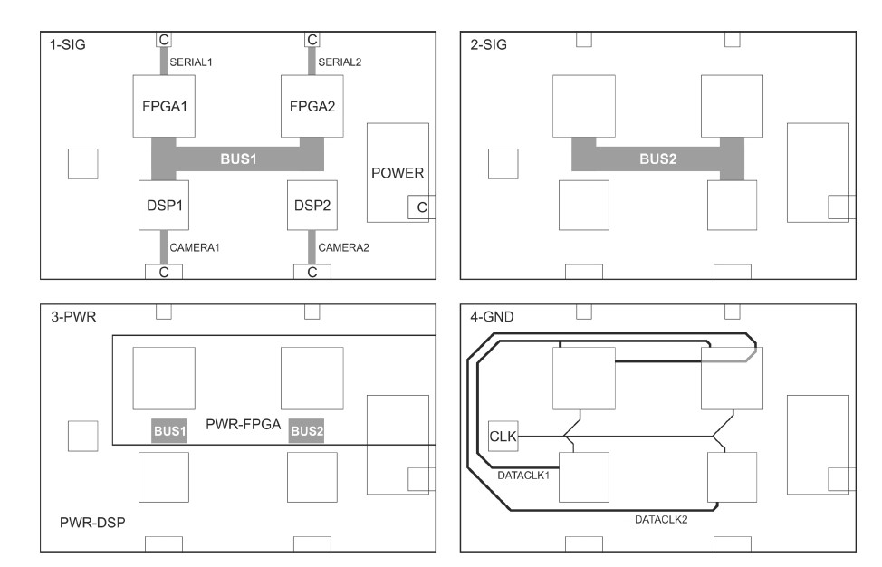
The design you are going to examine is a processing board for a machine vision system, which receives signals from two high speed camera modules. The data from each camera module is processed by a combination of a DSP processor and an FPGA. High bandwidth data buses (24 bits, clocked at 200 MHz) connect each DSP device to both FPGAs. Each of these data buses has 24 bi-directional data lines and its own data transfer clock (DATACLKn), sourced from the relevant DSP device. Processed image data are output from the board via a pair of high speed (5 Gb/s) serial links, using drivers located within the FPGAs. These serial links use differential pairs (LVDS). Figure 1 provides an overview of the design.
The design was started by an engineer who has since left the company and one purpose of today’s review is to establish the status of the project. The engineer’s notes on the design include the following summary of the layer stack and its use:
“The design fits into 4 layers as there aren’t that many interconnects. The FPGA data sheet recommends using interplane capacitance when using the serial transceivers so I’ve specified a 0.2 mm / 1.2 mm / 0.2 mm layer stack. This puts both signal layers a similar height above the reference plane, which is handy. I’ve kept all the clocks out of the way on the bottom layer as the FPGA data sheet says a low jitter clock is essential for the serial transceivers. The power plane is split to provide the FPGA and DSP supplies.”
Initial performance and electromagnetic compatibility (EMC) testing didn’t go well, as seen in this second extract from the engineer’s lab book:“I’m having problems with the serial transceivers. I see a high bit error rate. I initially thought it was an assembly problem – the PCB looks a bit warped - but it works fine if I lower the data rate. The data buses have problems at high speeds too. Looking at them on the logic analyser, some lines seem delayed or have slow rise times compared to my simulation. Preliminary EMC tests were disappointing too; it needed a fully shielded enclosure and ferrites on the cables to pass the emissions test.”
Assignment:
Following the second tutorial session, I will post a summary of problems identified with the existing design. Write a brief description of your personal final design (not necessarily that produced by your group during Activity 2). This should be no more than 500 words plus a diagram similar to Figure 1, which may be hand drawn as if in your lab notebook; I’m looking for concepts not presentation. You should provide technical justification for your design choices, especially around layer stack selection and use.
The Layer Stack of the Existing PCB Design
Checklist for High Speed Digital Design
Board construction and layer stack
- Are the layers mechanically balanced to avoid manufacturing problems?
- Is the layer stack appropriate (correct resources for design, no excess layers)?
- Is board level shielding present / adequate (if required)?
Component placement
- Has a defined IO region been implemented?
- Are any components placed inappropriately (e.g. too close to board edge)?
- Have clocks and high speed circuits been kept away from the IO region?
- Does the placement permit efficient routeing?
Signal routeing
- Are all signal layers adjacent to at least one reference plane?
- Do any signal traces cross reference plane discontinuities (splits or similar)?
- Have all high speed / potentially distributed lines been identified (LE/6, inches>ns)?
- Are all high speed lines tightly coupled (< 0.25 mm) to at least one reference plane?
- Are all high speed lines shielded within reference plane layers?
- Have appropriate controlled impedance routeing and termination techniques been applied to any distributed lines?
- Have return paths been provided at changes of reference plane (via or cap)
Clocks and other critical nets
- Has additional care been taken with critical nets (minimal length, optimal routeing)?
Power and grounding
- Does the board include appropriate power and ground planes?
- Are power and ground planes tightly coupled for low inductance / high interplane capacitance (if needed)?
- Are multiple ground planes present / required?
- Are the enclosure (if conductive), board and cable grounds connected in the IO region?
- Are any heatsinks, etc. grounded?
- Is adequate capacitive decoupling present at device (power pin) and board (bulk caps) level?
- Are power supplies regulated at board level?
Discussions
Become a Hackaday.io Member
Create an account to leave a comment. Already have an account? Log In.