The figure below shows the existing PCB Design:
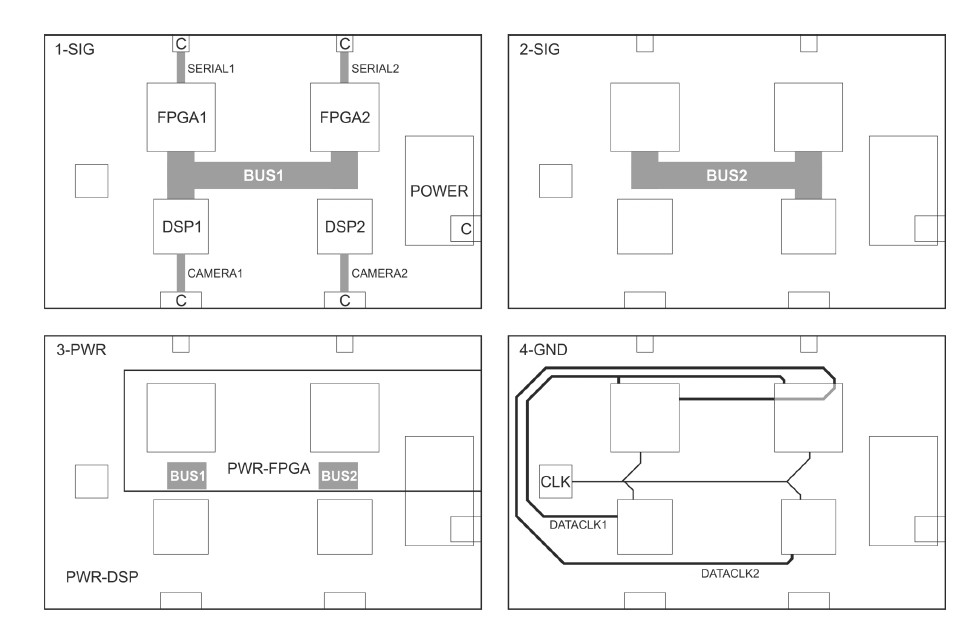
As a result of the design review, a number of changes needed to be made in order to improve its test results.
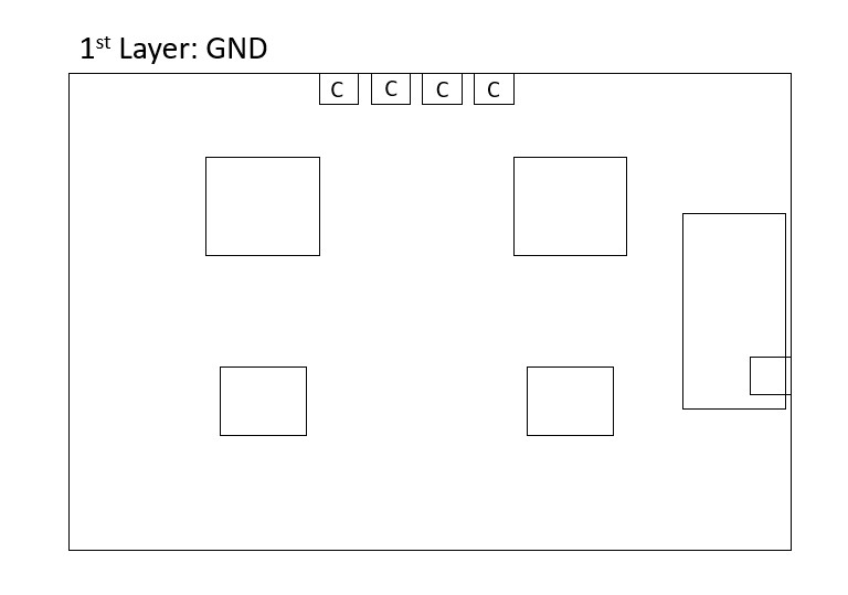
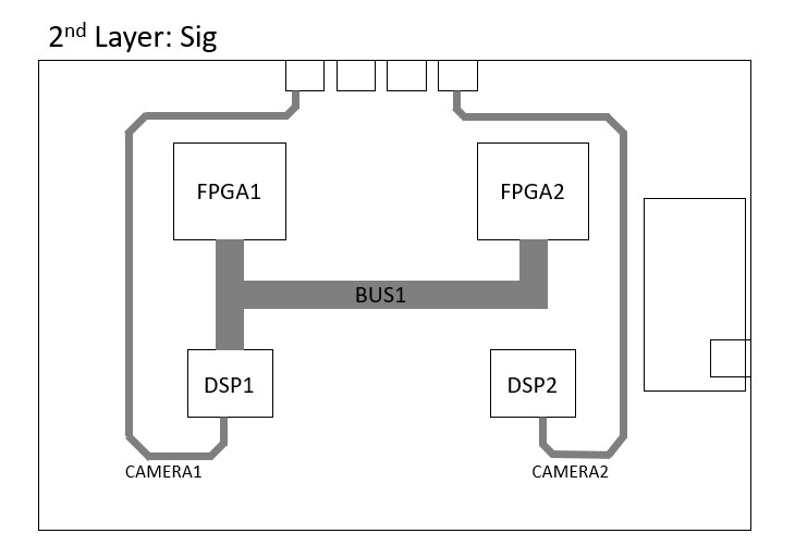
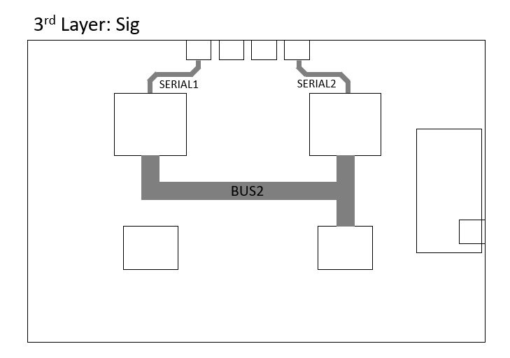
First of all, a layer stack selection of 8 layers is made. Although it seems like the costs are increasing at the first glance, once the cost of the shielded enclosure to reduce the emission is considered, making the shielding at the PCB level by increasing the number of layers is actually a better choice. Consequently, the high speed signal layers are placed in layers 2 and 3. They are enclosed by GND and Power planes to provide the required shield for the EMC tests.
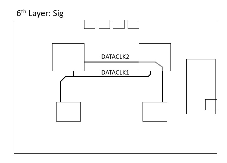
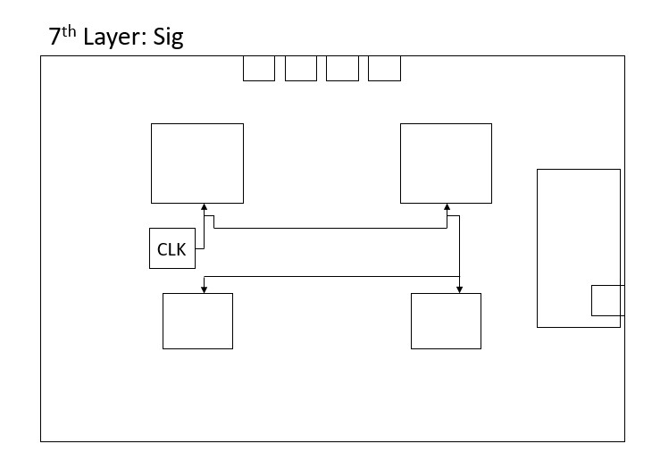
Additionally, branching of the CLK is avoided by applying the daisy chain method, by doing so the track length is increased which is undesired but in return the noise is reduced. The DATACLK 1 and 2, are intentionally kept as short as possible to avoid the delay and parasitics caused by the excess trace length. Both of the CLK and DATACLK signals are placed within the PCB and isolated from other high speed signals.
As it is pointed out by the engineer that the there is a delay or slow rise time in the lines of data buses, mainly due to the signal plane not being adjacent to a reference plane. In addition, due to high inductance the rise time is slowed down. Therefore, an adjacent reference plane is placed next to each high speed signal layer.
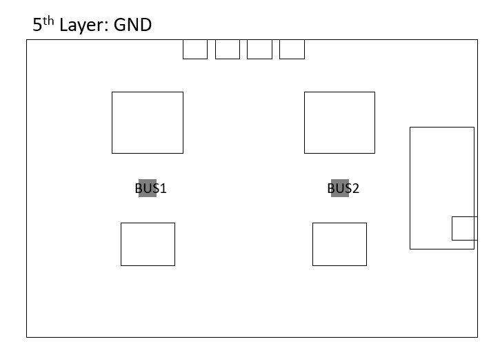
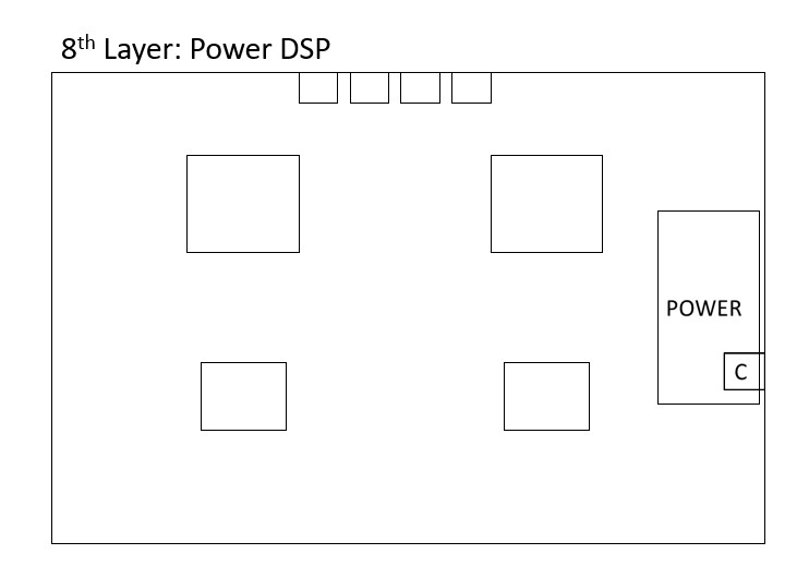
Also, the GND plane should not be interrupted to allow the flow of the return current freely. Hence, the GND planes adjacent to the signal layers are deliberately left empty. Furthermore, the VCC (Power) and GND planes are closely coupled together by placing them next to each other, reducing the inductance.
An IO region is defined to minimise the effect of the potential difference engendered by the returning currents flowing on the non-ideal (the impedance is not zero) GND planes.
The engineer has also noted that the PCB looked slightly warped which indicates that it is mechanically imbalanced. In order to solve that problem, the 4 ICs and other PCB components are located with care to permit efficient routeing and to avoid PCB warpage.
In non-ideal cases, the signal that flows through the distributed lines of the PCB is not fully absorbed by the load and a certain amount of the signal is reflected which amplifies or cancels out the original propagating signal. This phenomenon causes ringing which affects the signal integrity and produces anomalies in the signal as well as the circuit. Controlled impedance routing and termination techniques are used to match the impedance of the two ends of the trace by altering its dimensions consequently, the effects of ringing are minimised.
The new design is as follows:

Discussions
Become a Hackaday.io Member
Create an account to leave a comment. Already have an account? Log In.