 agp.cooper
The SUBLEQ Interpreter
Wikipedia presets the following SUBLEQ pseudocode:
 int memory[], program_counter, a, b, c
 program_counter = 0
 while (program_counter >= 0):
     a = memory[program_counter]
     b = memory[program_counter+1]
     c = memory[program_counter+2]
     if (a < 0 or b < 0):
         program_counter = -1
     else:
         memory[b] = memory[b] - memory[a]
         if (memory[b] > 0):
             program_counter += 3
         else:
             program_counter = c
In my case signed integers and a stopping condition are not required:
 int memory[], program_counter, a, b, c
 program_counter = 0
 while (true):
     a = memory[program_counter]
     b = memory[program_counter+1]
     c = memory[program_counter+2]
     if (memory[b] > memory[a]):
         memory[b] = memory[b] - memory[a]
         program_counter += 3
      else:
         memory[b] = memory[b] - memory[a]
         program_counter = c
A Schematic for an 8 bit SUBLEQ CPU
The schematic considers the scaling up to any word width (i.e. 8, 16, 14 or 32 bit).
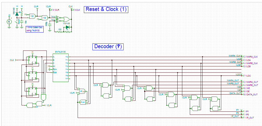
The Decoder
The first step is the Reset, Clock and Decoder logic.
Initially I used Logic Friday to develop a schematic but the schematic when modelled in Tina TI was badly glitched. I did fix it with D-latches but the chip count was highe than I have achieved using manual methods.
Here is a schematic for my decoder:
And here are the signals:
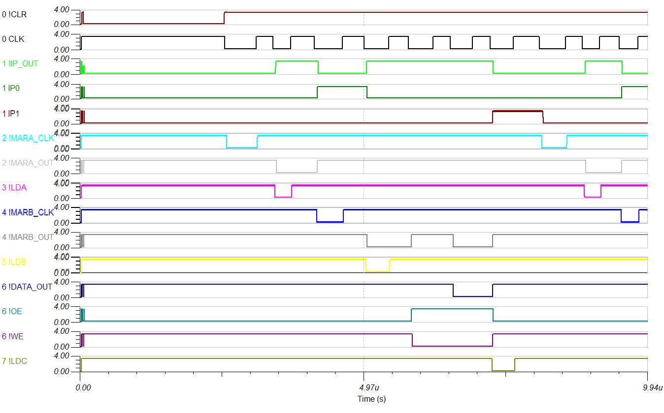
Static RAM Write Timing
I have been using a particular static RAM timing cycle that up until I blew up a RAM chip I thought was okay (i.e. after the !WE pulse the RAM chip did't care less with regard to memory conflicts - Wrong!).
So after carefully reviewing the RAM datasheet I now use the above !DATA_OUT, !OE (not used on my RAM chips) and !WE. !DATA_OUT waits until !WE disables the RAM output.
The Instruction Pointer
The instruction pointer uses an ADDER to increase the base memory address rather than a COUNTER. The DECODER provides the address increments (signal IP0 and IP1):
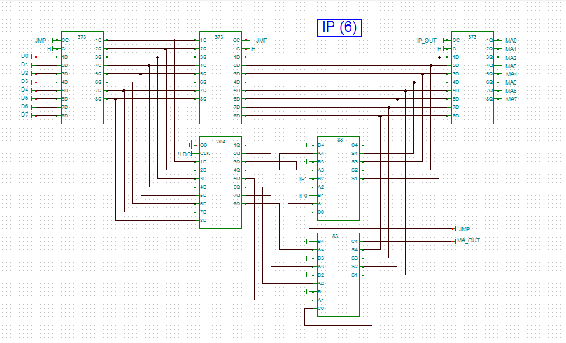
If "!JMP" is low then the Address C replaces IP (the 374) upon the LDC signal. Else the IP is incremented by 3 (via the ADDER and the Carry In).
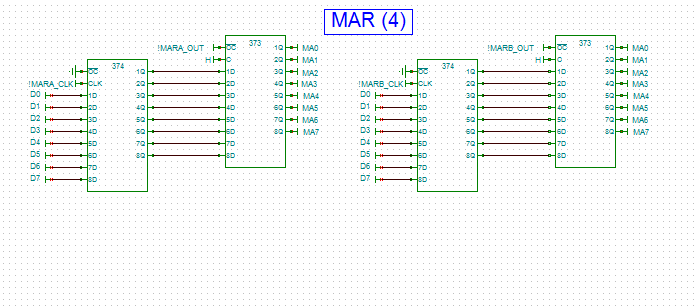
The Memory Access Registers
The Memory Access Registers (MAR) hold the fetched memory address that is then used to load the pointed values. (much like my Weird CPU):
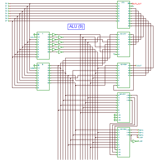
The ALU
Its not much, it just subtracts A from B and tests for a JMP (i.e. A >= B):
The schematics need review and I have not considered the Memory/Input/Output decoder or the Front Panel yet. I am also consider changing the signal logic to use 373's rather than 374's.
The number in the labels of each drawing is the number of chips so the CPU will require 29 chips.
AlanX
Discussions
Become a Hackaday.io Member
Create an account to leave a comment. Already have an account? Log In.