 Maarten Janssen
Continuing my VideoWRITER autopsy, this time I want to learn more about its memory configuration. Last time we already saw that the system holds 16kb of RAM and a total of 64kb of ROM, leading me to believe that we may also find some bank switching circuitry today. I did some poking around with my multimeter on continuity to trace the various signals and drew some schematics on paper.
Chip Selects
I will start by reverse engineering the chip select lines of the memory. This should give us a rough idea of the system's memory map as well since usually a particular memory chip is selected based on its address in the memory map. I will start from the /CE pin of ROM A. Running the other probe of my multimeter along the pins of other chips on the board until I hear a beep. And hey, what do you know it starts beeping at the output of an AND gate. Now to trace the two inputs of this gate... Turns out they go to two outputs of an 74139 (a 1 out of 4 selector).

The 139 has A14 and A15 from the CPU as its address inputs, so this means that the memory is divided up into four blocks of 16kb. The /E (enable) line of the 139 goes to the CPU's /M (memory select) line, so the 139 is active when the CPU wants access to the memory. After tracing the circuit I come to the following memory map in the table below. ROM A is active when either /Q1 or /Q2 of the 139 is active, ROM B is active on /Q2 and the RAM on /Q3, but the RAM is not as straightforward as the ROMs. More on that later...
| A15 | A14 | Memory |
| 0 | 0 | ROM A |
| 0 | 1 | ROM A |
| 1 | 0 | ROM B |
| 1 | 1 | RAM |
The Address Bus
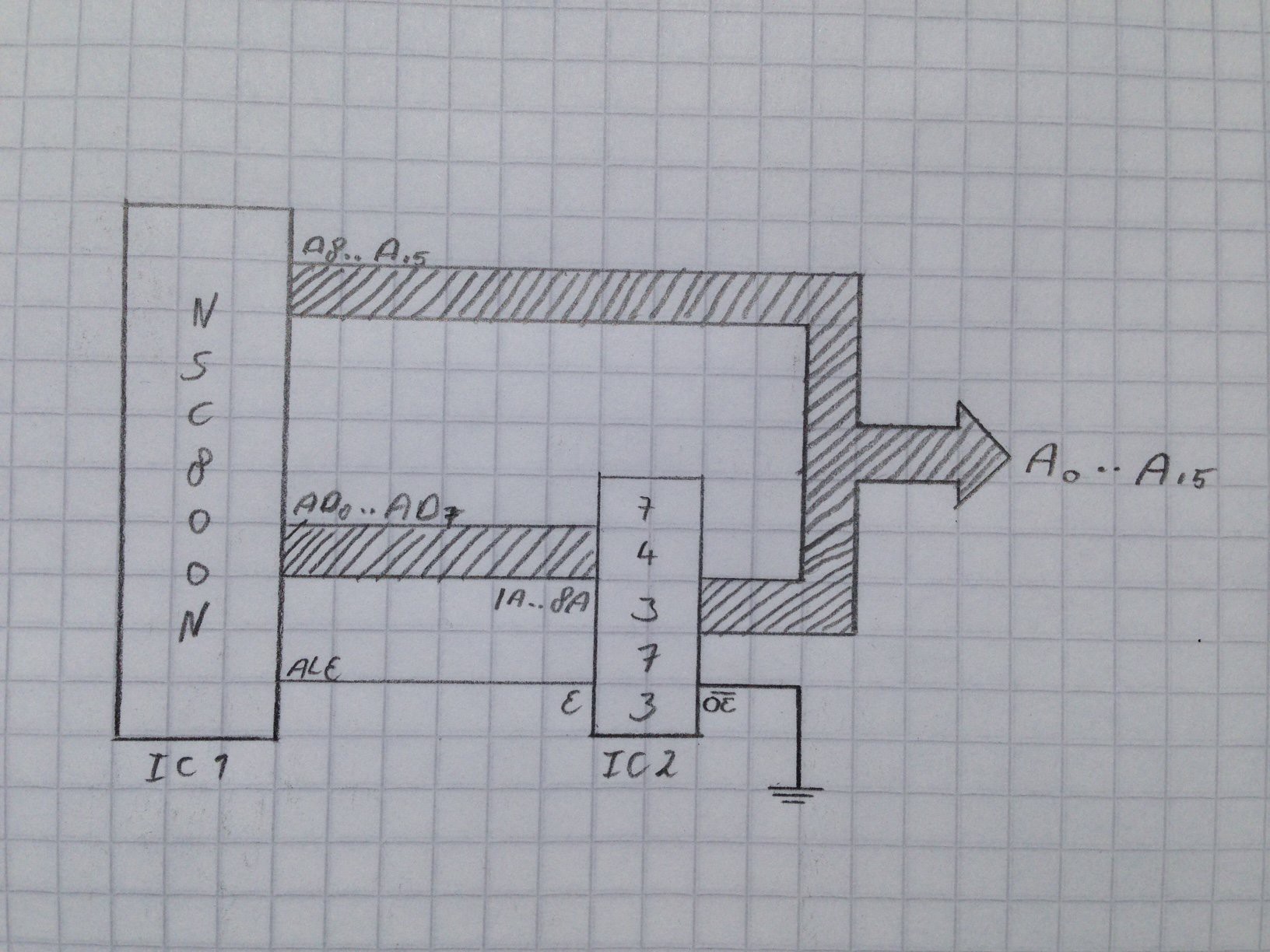
Let's now take a look at the address bus of the VideoWRITER, because it's a bit more involved than that of a normal Z80 system. As I noted last time the NSC800N shares the lower half of its address bus with its data bus. So in order to separate the two what they did was use a 74373 (an 8-bit latch) to hold the lower 8 bits of the address bus. The inputs of the 373 connect to AD0 through AD7 of the CPU and the CPU's ALE line is connected to the latch pin of the 373. Thus when the CPU's Address Latch Enable line goes high the lower half of the address is copied into the 373. The /OE of the 373 is tied to ground, so it's always holding the current address on its output.
From now on I will refer to the address bus as the combined output of the 373 and upper address lines of the CPU as A0 through A15.
ROM Addresses
Now we know how the address bus is set up we can take a look at how the ROMs are connected. Starting with ROM A we find nothing unusual. A0 through A14 are tied together as you'd expect. For ROM B A0 through A13 are tied to the address bus, which makes sense since it can only use 16kb according to the memory map we found earlier. What about A14? Does it go to Vcc or ground to disable one half of the memory? Nope. It goes to pin 39 (PC2) of the D8156 IO controller. That means that the upper and lower 16kb of ROM B can be exchanged in software and the bank switching mystery is solved :).
RAM Addresses
This is going to be the complicated part of this log. We saw that the VideoWRITER uses two 16k x 4 DRAM chips for its RAM. We also saw that in order to make a full 8-bit data bus one chip serves the upper four bits and the other the lower four. This means that all the signals going to the chips are the same for both.
To select an address of these DRAMs you need to first select a row address, followed by a column address. In this design this is implemented using two 74157s (2 to 1 line data selectors). These are used to output the row or the column address depending on the select input. To know when the row or column is selected we have to go back to schematic 1. Above the RAM /WR output you see that there is another output going to the select line of the first 157. Following the logic gates from the schematic, worked out below, we can deduce that when /Q3 is low a column address is selected and when /Q3 is high a row address is selected.
| /Q3 | /RD | /WR | Select | |
| 0 | 0 | 0 | 0 | Impossible state |
| 0 | 0 | 1 | 0 | |
| 0 | 1 | 0 | 0 | |
| 0 | 1 | 1 | 0 | |
| 1 | 0 | 0 | 1 | Impossible state |
| 1 | 0 | 1 | 1 | |
| 1 | 1 | 0 | 1 | |
| 1 | 1 | 1 | 1 |
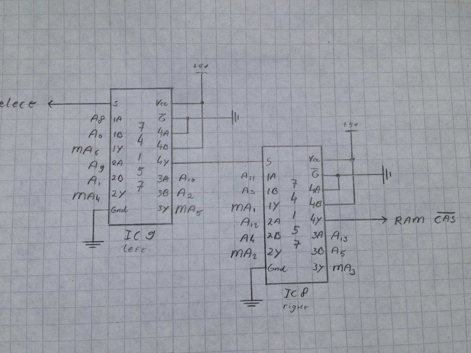
When I was tracing the outputs of the 157s I found that only 6 out of 8 are being used as addresses MA1 through MA6 of the DRAMs and that MA0 and MA7 of the DRAMs are connected to A6 and A7 of the address bus. These 48416 DRAMs have 8 rows and 6 columns, so only 6 lines need to be switched and the two remaining lines can be connected statically to the address bus since they do not affect the column selection.
What surprised me most was the order in which the address bus lines are connected to the DRAM's address lines. There seems to be no logic there looking at the row / column map I drew in the schematic. Still it works fine. The data ends up in RAM albeit not as a neat continuous stream.
Another thing I found interesting about how these 157s are used is how the select line of the first 157 cascades through the schematic to form the select line of the second 157 (through output 4y) and finally the /CAS line of the DRAMs through 4Y of the second 157.

The DRAMs have no separate /CE line like the ROMs. As far as I understand DRAMs these chips are able to read or write when their /CAS is low. Looking at the logic from schematic 1 this is exactly what it does since when /Q3 is low /CAS will be low as well. The row address of the RAM is set when the CPU's ALE is low and when the CPU is not being reset.
I think that about covers the way they implemented the VideoWRITER's memory. Next time let's do the same for the IO.
Discussions
Become a Hackaday.io Member
Create an account to leave a comment. Already have an account? Log In.