 Maarten Janssen
It's time to start looking at the IO map of the VideoWRITER. With the help of my trusty multimeter I have been probing around the main board and I've drawn the following schematic.
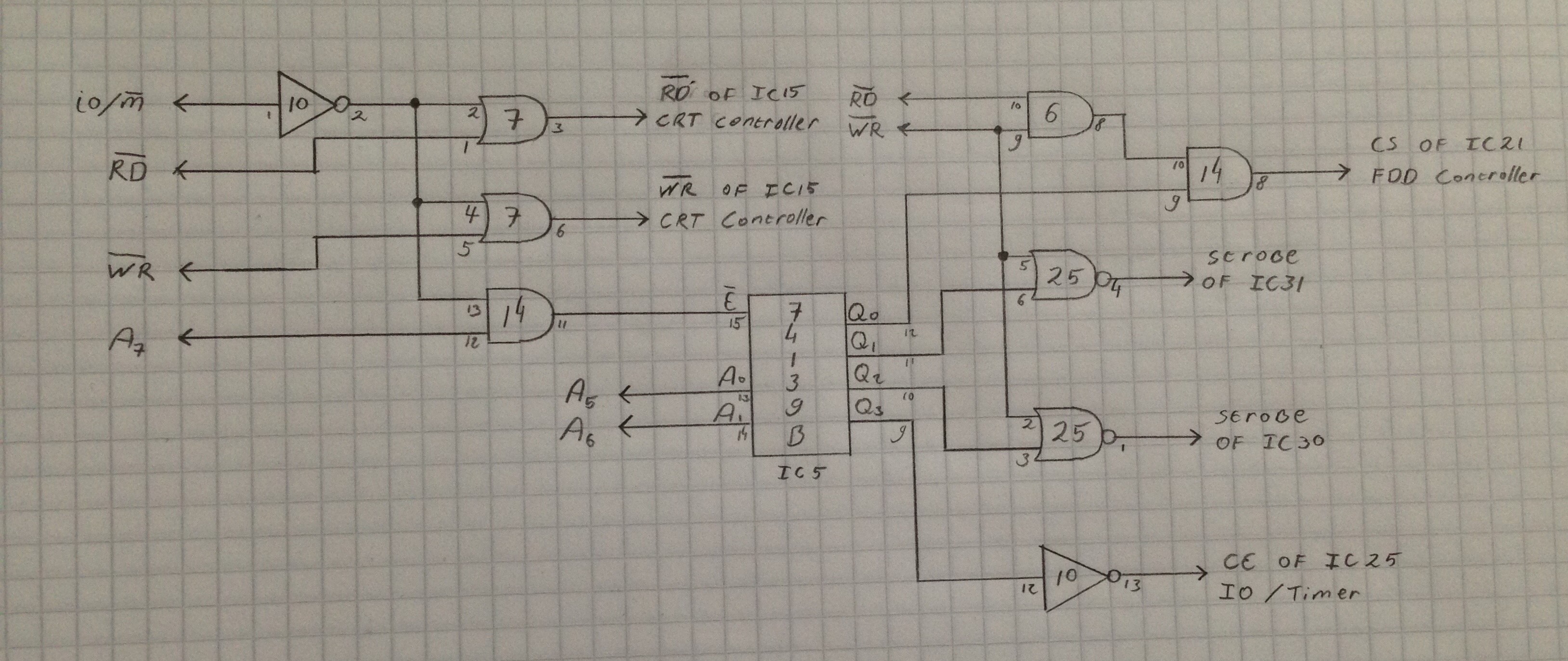
Let's start looking at the left part of the schematic before the 74139. This is where the /RD and /WR signals for the video controller (VDP) are generated. Notice that there is no chip select signal for the VDP in this schematic. This puzzles me since the only signal going to the VDP that comes close to a /CS signal is the CPU's ALE. But that means that any IO operation also ends up at the VDP as far as I can tell now. Let's park this for now and continue with decoding the rest of the IO.
The rest of the IO addresses are decoded using the second half the 74139 we saw before when decoding the memory. This half of the 74139 is enabled when we're doing an IO operation and A7 is low. It looks like A7 is responsible for choosing between addressing of the VDP and other IO. A6 and A5 determine the device that is selected by the 74139. This decodes to the following:
| A7 | A6 | A5 | Selected device |
| 0 | 0 | 0 | Floppy Disc Controller (FDC) |
| 0 | 0 | 1 | Latch B (IC31) only when /WR is active also |
| 0 | 1 | 0 | Latch A (IC30) only when /WR is active also |
| 0 | 1 | 1 | IO / Timer (IC15) |
| 1 | x | x | Video Display Controller (IC15) |
Just a thought... Could A7 be used as an active high chip select line for the VDP? It's hard to tell without the datasheet of the NCR 7250, but it would make sense unless there is some magic happening with the ALE line going to the VDP chip. This is something to look into for the next log...
CPU Signal Lines
While we're at it let's take a closer look at the signal lines coming from and going to the CPU. That allows us to say something about the various interrupts that are generated in the system as well. Once again I buzzed-out the schematic and drew it on paper.
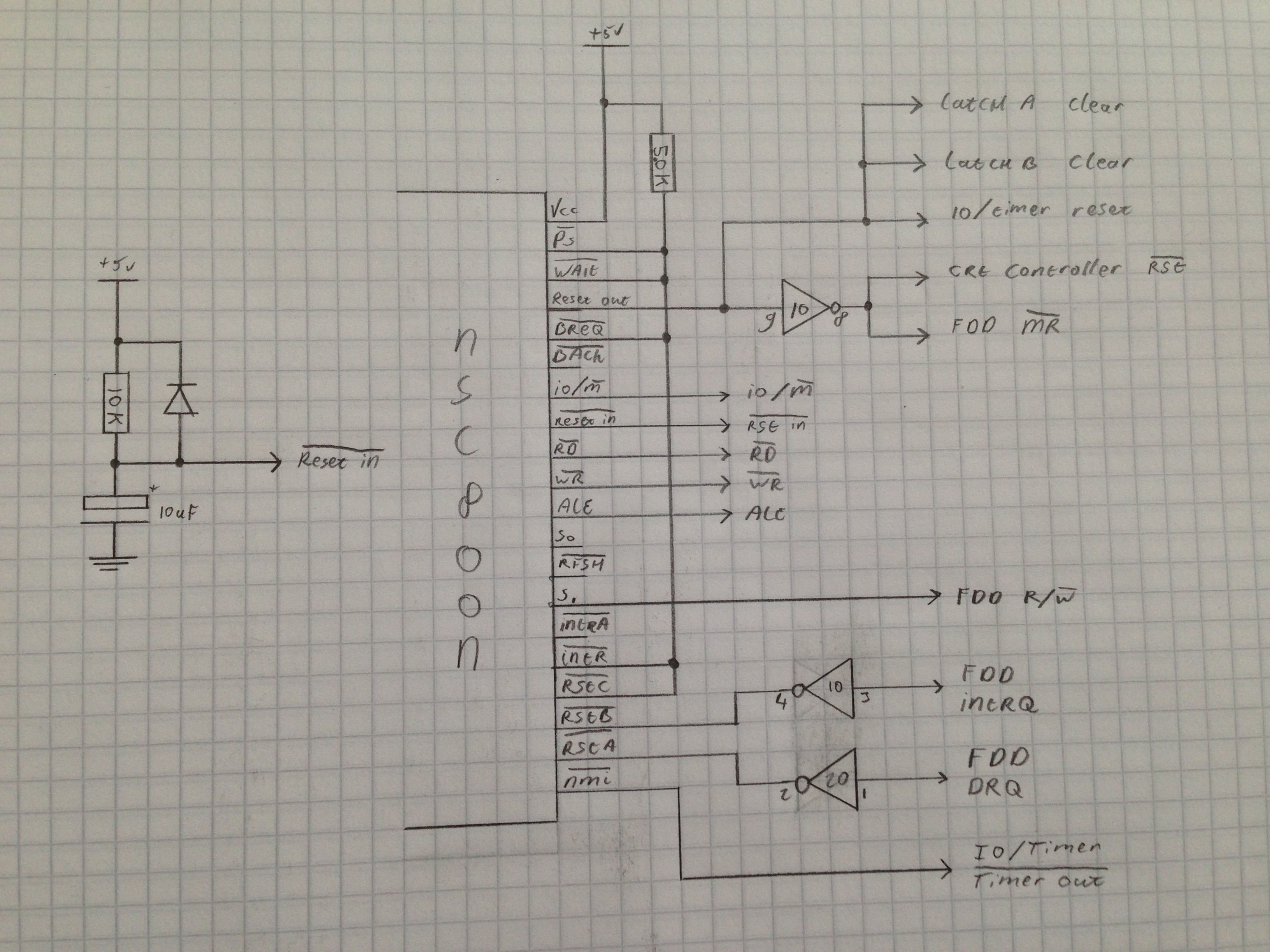
Reset
Starting off with the reset circuitry, the CPU has a /RESET IN and RESET OUT line. The /RESET IN line is what resets the system when pulled low. The inverse of this signal is put on the RESET OUT line to generate a reset pulse for the various devices connected to the CPU. In our case it resets all the IO chips FDC, VDP, IO / Timer and Latches when power is applied.
Interrupts
Let's continue at the bottom of the chip now where the various interrupt signals come in. Starting off with the /NMI (Non Maskable Interrupt) pin. The NMI works the same as for a Z80. When interrupts are enabled and this pin is pulled low the CPU will jump to an interrupt service routine at address 0x66. In case of the VideoWRITER the /NMI signal comes from the timer output of IC25 (IO / Timer). Every time the timer rolls over an interrupt is generated.
In addition to a Z80 compatible /NMI the NSC800N also has a Z80 compatible mode 1 interrupt that jumps to 0x38 when /INTR is pulled low, but this is not used in the VideoWRITER.
Besides these two interrupt signals the NSC800N has three restart signal inputs /RSTA, /RSTB and /RSTC that make the CPU jump to 0x3C, 0x34 and 0x2C respectively. The VideoWRITER uses the first two and they are controlled by the floppy disc controller. With /RSTA the FDC tells the CPU about the status of its data register and /RSTB tells the CPU that the FDC has completed its last command.
Machine states
The final signal I want to highlight is the S1 line. Together with S0 these determine the bus status. As you can see this controls the R/W line of the FDC. But why is S1 used instead of the /RD and /WR lines only for the FDC? This is not clear to me. Using the S0, S1 and IO/M lines is probably the intended way of decoding memory and IO read / write states, but using other lines has the same effect. Maybe the designers were just trying it out and said 'screw it!' for the other devices and went with a Z80 like way of decoding read / write states. Anyway at the NSC800N datasheet and the table below it shows that S1 can be used as an IO read signal, but only if there is also an IO select signal going to the device.
| S0 | S1 | IO/M | /RD | /WR | Machine Cycle |
| 1 | 1 | 0 | 0 | 1 | Opcode fetch |
| 0 | 1 | 0 | 0 | 1 | Memory read |
| 1 | 0 | 0 | 1 | 0 | Memory write |
| 0 | 1 | 1 | 0 | 1 | I/O read |
| 1 | 0 | 1 | 1 | 0 | I/O write |
| 0 | 0 | 0 | 0 | 1 | Halt |
| 0 | 1 | 0 | 1 | 1 | Internal operation |
| 1 | 1 | 0 | 1 | 1 | Interrupt acknowledge |
That's all for now. In the next log we will start to take a look at the mysterious NCR 7250 display controller.
Discussions
Become a Hackaday.io Member
Create an account to leave a comment. Already have an account? Log In.