Close
0%
0%

Over-engineered LED strip controller

Way too much stuff to light my garage MY way.

Similar projects worth following
I've put up the usual 12V LED strips to give more light in my garage. Like everybody else, I'm going to make a custom controller for those lights. This is part practical, part aesthetics, and part learning exercise.

EDIT: A drastic change of approach. See the final project log entry for details.

My garage is 20 ft x 30 ft. (That's about 0.01 US [Imperial] football fields and an indeterminate number of metric [FIFA] football pitches.) The original lighting in there is 3 connected ceiling-mounted sockets. That's enough light to walk through there without risking your life, but it's very poor lighting for actually doing anything in that garage.

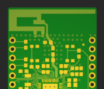
It's easy to find many descriptions of people putting up inexpensive 12V LED strips in garages or other places. So, hey, me too! I'm not bothering with describing much of that part of the project because there is nothing special about my take on it. This project is about the controller I am making for it.

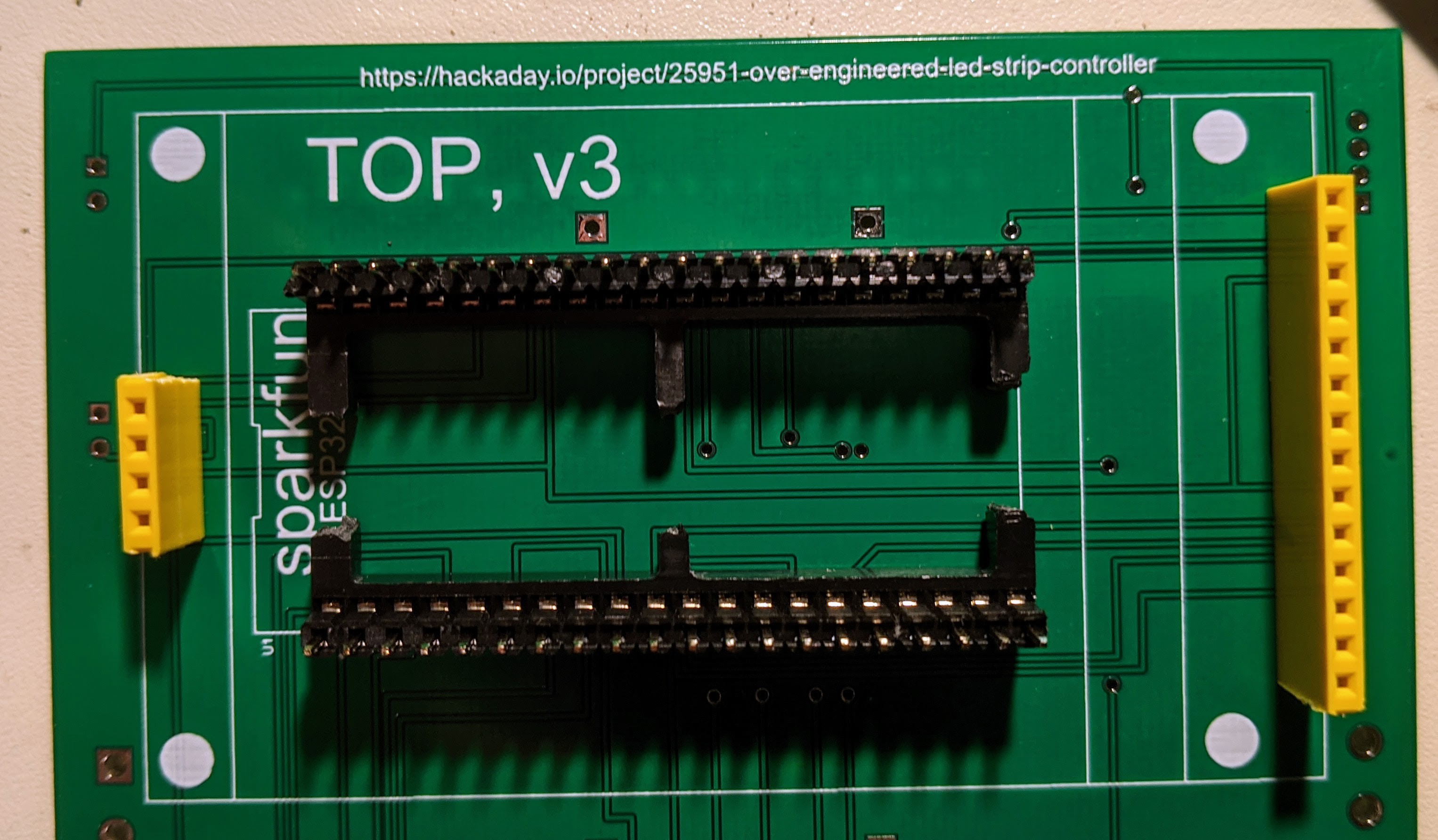
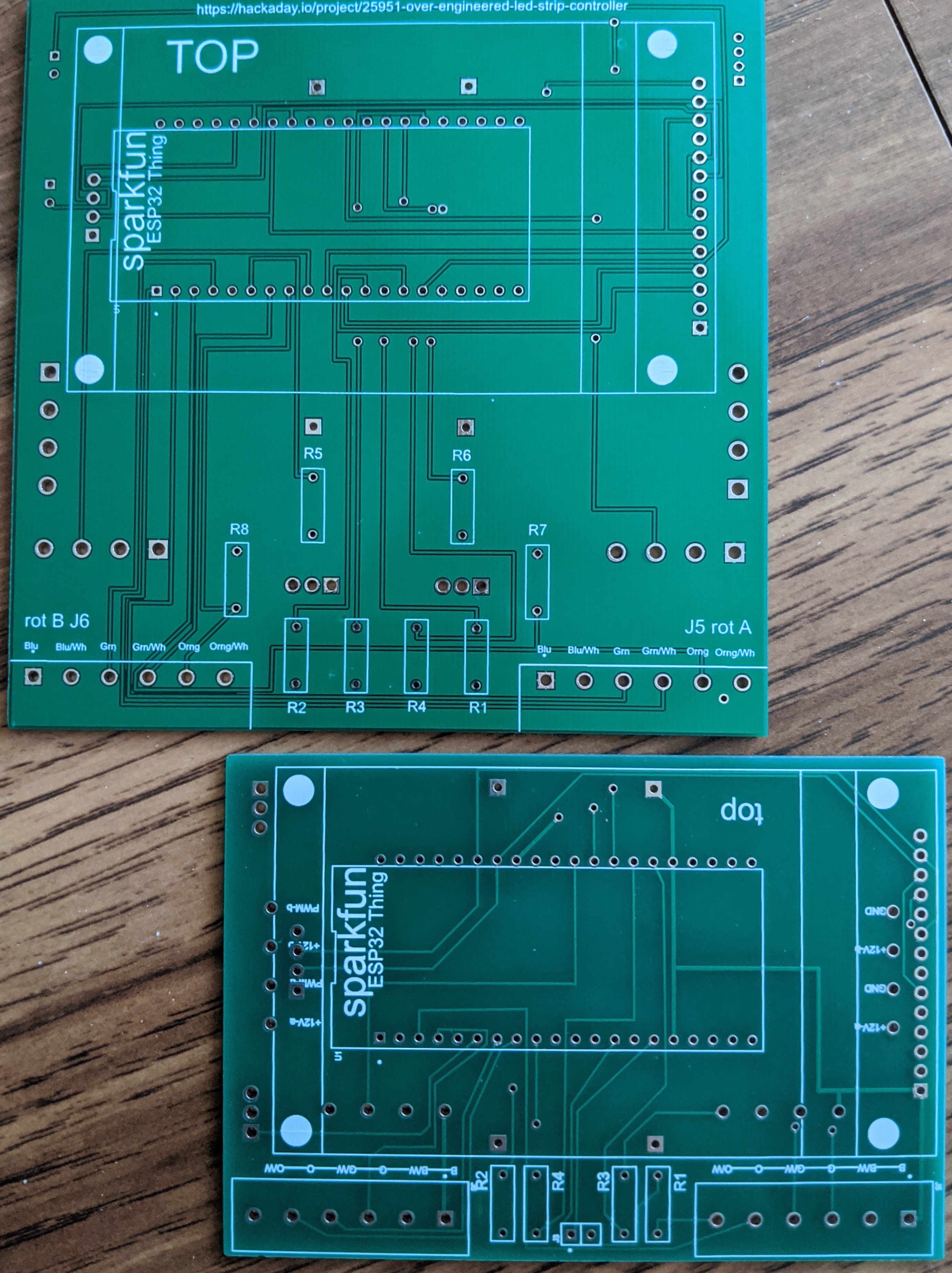
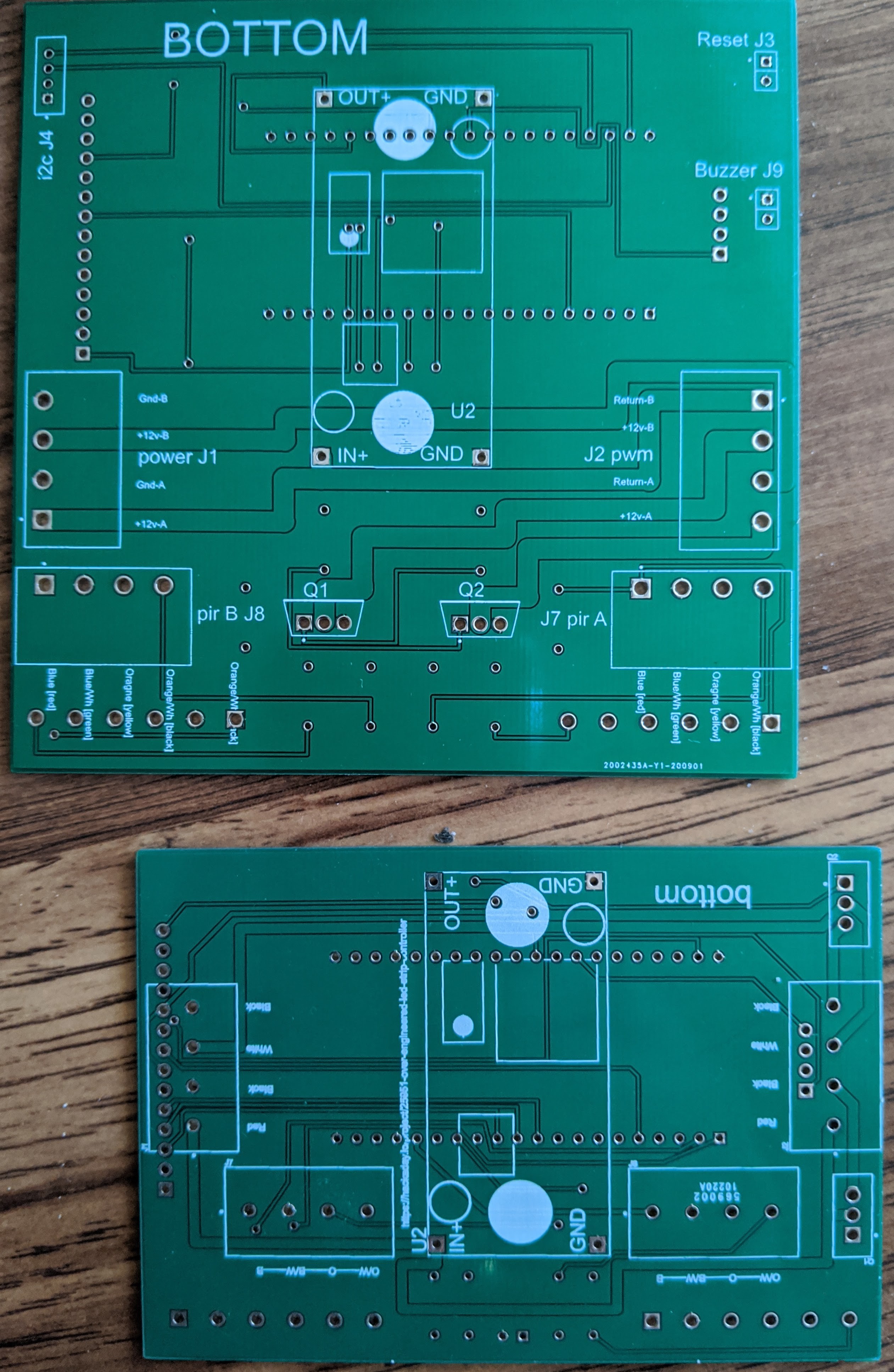
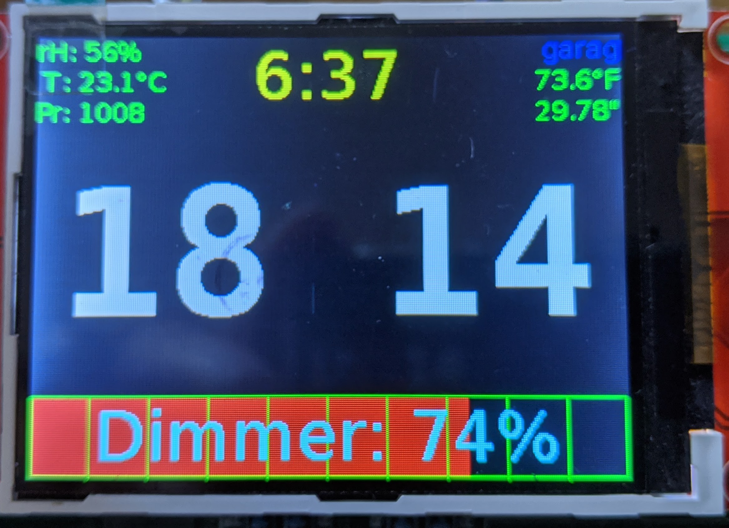
Here's a high-level view of the features:

  • Two remote passive infra-red (PIR) motion detectors to keep the lights from timing out while someone is present.
  • Two remote control knobs consisting of rotary encoders with built-in momentary switches. These are both on/off switches and also dimmer controls.
  • The PIRs have LEDs for debugging/feedback.
  • The control knobs have LEDs for easy location in the dark.
  • Sensors for temperature, air pressure, and relative humidity.
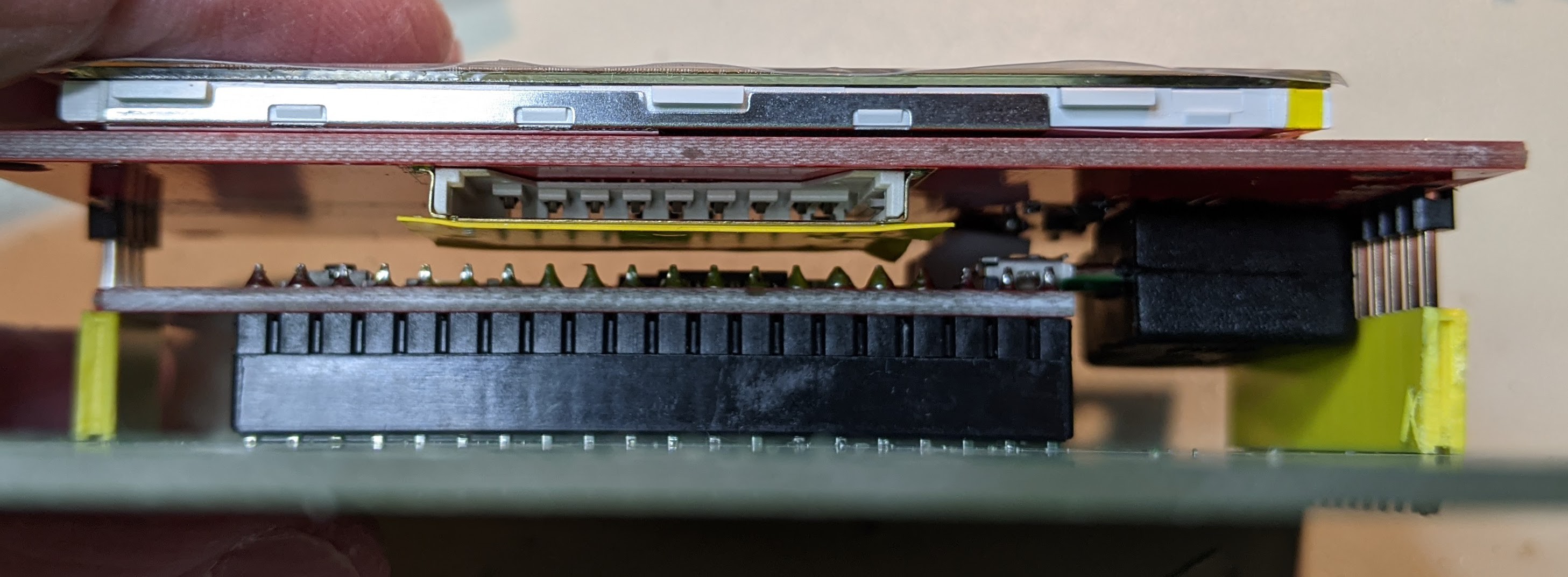
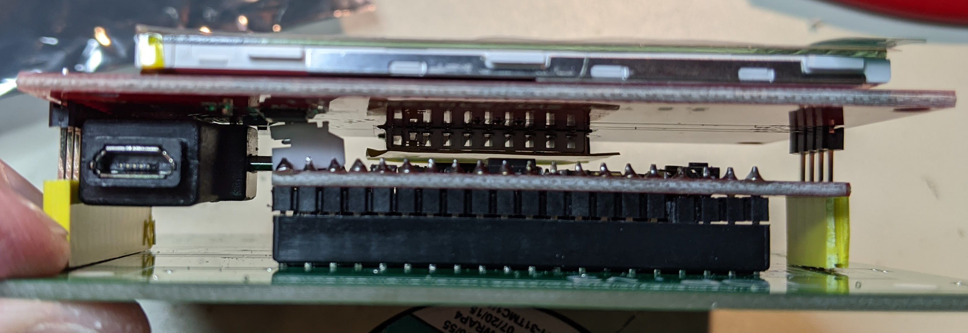
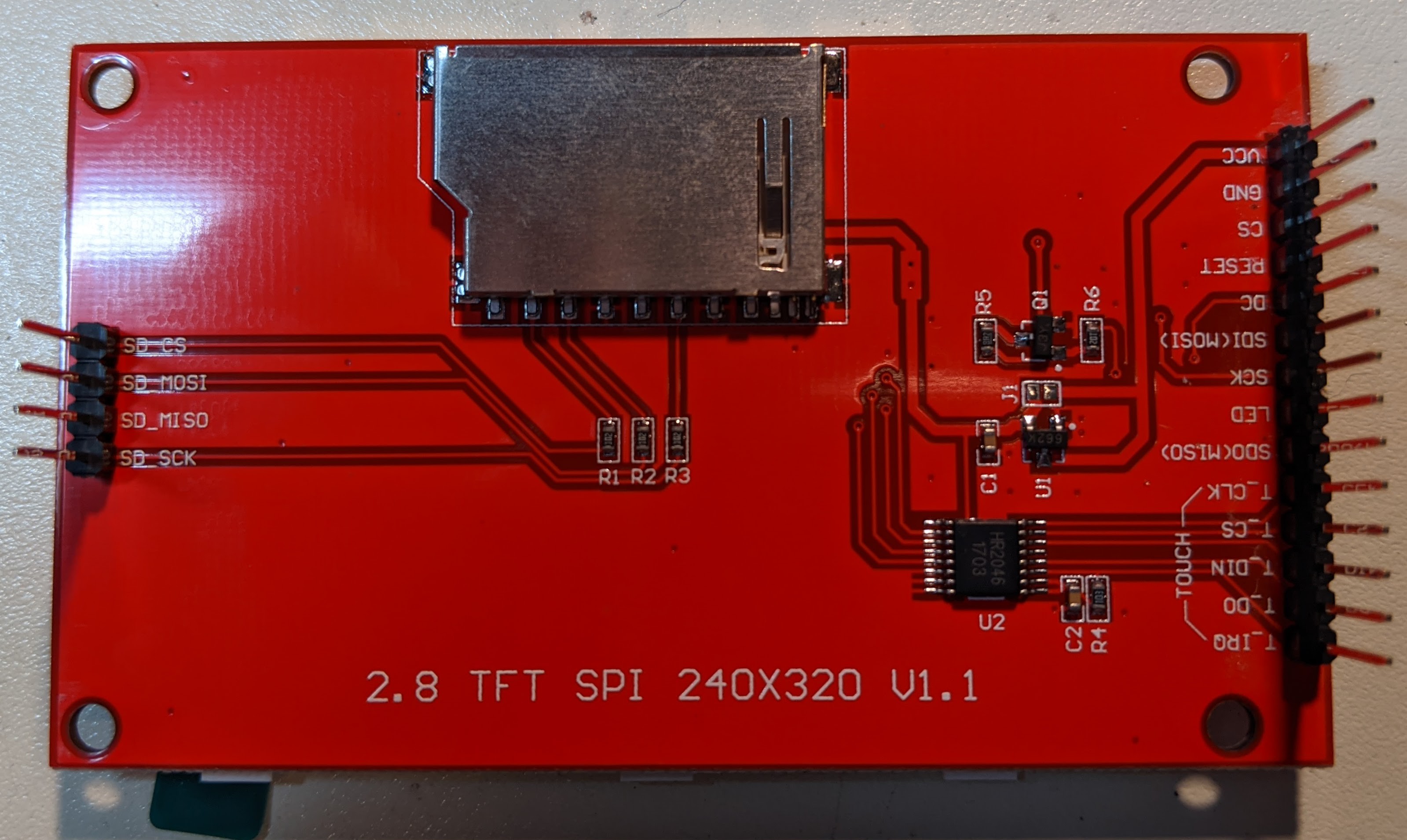
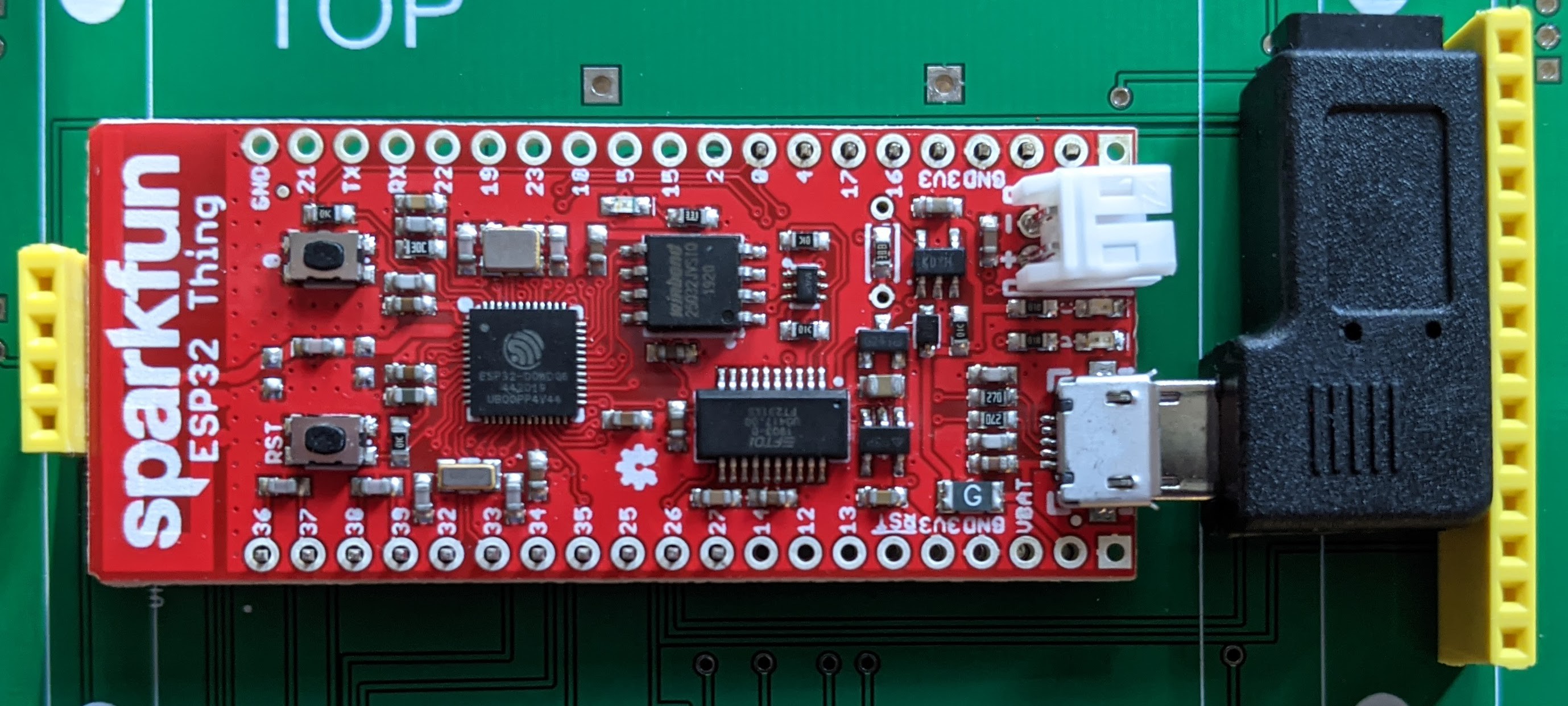
  • A built-in touchscreen display. (Not planning to implement the touch part in software.)
  • SD card slot for possible data recording. (Not planning to implement this in software.)

Creative Commons License
Over-engineered LED strip controller by WJCarpenter is licensed under a Creative Commons Attribution-ShareAlike 4.0 International License.

garmotion.yaml

ESPHome configuration file that I ultimately used.

x-yaml - 6.11 kB - 09/05/2021 at 19:51

Download

garag.yaml

This is the ESPHome configuration file that was mentioned in some project logs. It was still a work-in-progress when I changed the entire approach. I can't guarantee anything in here works correctly.

x-yaml - 22.12 kB - 09/05/2021 at 19:53

Download

  • 1 × SparkFun ESP32 Thing https://www.sparkfun.com/products/13907 (NOTE: NOT the ESP32 Thing Plus)
  • 1 × TJCTM24028-SPI TFT display 320x240 2.8 inches
  • 1 × 90 deg micro-USB connector adapter connects to microprocessor board (optional); see build notes for orientation
  • 30 × meters (approx) of 3-pair solid wire telephone cable Length will depend on the actual placement of remotes
  • 1 × DC-DC 3A Buck Converter Adjustable Step-Down Power Supply Module LM2596S actual power draw is well under 1A # 3v3; spacing of pads on PCB: 0.8 in x 1.8 in

View all 21 components

  • Winding it down: the after-action report

    WJCarpenter09/05/2021 at 19:50 0 comments

    "Thanks for your valuable service. You have made immense contributions. You are well on the way  to creating something great. Unfortunately, due to ... mumble, mumble, mumble ... we are forced to make some hard decisions. We are re-prioritizing our efforts in different areas. To better serve our customers, re-align with our stakeholders, blah, blah blah...."


    Chairman: Doctor, you are genius!

    Dr. Poppover: Of course.

    Chairman: You are national hero!

    Dr. Poppover: Natch.

    Chairman: You are under arrest!

    Dr. Poppover: Eh, why?

    Chairman: You know too much.

    Dr. Poppover: Oh.


    Well, I learned (or re-learned) a heck of a lot by working on this project over the course of several years. I've decided to break my pretty balloon and put all my toys away, at least for this project. Some things have changed over the 4+ years since I started it, and I'm not even talking about the crazy number of times I changed my mind about details of the project itself.

    • After a few years of service, the inexpensive LED strips I bought have started to show small areas of blinkies and fade-out. I haven't had to replace any sections yet, but I've become skeptical about their lifetime.
    • Due to the continued accumulation of detritus and the consequent narrowing of walking pathways in the garage, the need for good and automatic lighting is becoming more and more important to me every day. I'm afraid they might find me under a heap of non-automotive possessions before I can finish the project.
    • Alternatives to LED strip lighting have become better, cheaper, all-around nicer in recent years. I bought dimmable LED tube replacements for some fluorescent bulbs probably more than 10 years ago, for an outrageous price, and their dimmability was pretty horrible. My local utility company now sells 4 foot dimmable LED tubes for US$5 (including a US$2 rebate per tube). They are "direct replacement" so can be used with or without ballast. I have some, and they are excellent.
    • While wandering through my local home center, I saw a clearance item of some 4 foot tube fixtures. Each can hold a pair of tubes. They were normally around US$35 (comparable to others not on clearance), and the clearance price was under US$7. As a Hackaday reader, it is my sworn duty to scoop up such bargains whether I need them or not. I visited a couple other locations of the same home center and bought all I could find. (I put one of these up in my basement where there was just a bulb before. Now I can see all the spiders. Yikes.)

    The most important thing that changed, however, is that I have switched my approach to home automation from being a series of one-offs, which are a combination of learning experience and disaster in the making, to a more organized approach. My weapon of choice now is Home Assistant, a widely used open source project. I got interested in this approach when I started to look into how I could keep historical records of things like temperature readings and then make cool visualizations of them. In theory, I could do all that from scratch and/or by cobbling together various off-the-shelf things, but who has that kind of time?

    (An aside about Home Assistant. They have a sort of middle-ground problem. There are tons of things you can do by just following their recipes or click-this-click-that in the web UI. They also have a very sophisticated architecture that makes extremely complex things possible without requiring fundamental changes in the framework. The middle ground problem is that there is a hard road in getting from that first stage to the last stage. If you are a programmer and are willing to work at it, you can figure it out.)


    I put the project to bed by implementing what I needed in a different way. This long posting describes what I did.

    I installed the motion sensors as originally planned. I ran the wires a while back, and they have just been dangling in the air since. You need three wires...

    Read more »

  • Grove connectors

    WJCarpenter09/20/2020 at 22:54 0 comments

    I didn't notice this until I was trying to place the headers for the I2C bus. I had intended to use the footprint for a 1x4 100 mil pitch male header strip. Without noticing, I selected a footprint that was 2.0 mm pitch. Although that is definitely a mistake, I can pretend it was intentional.

    I routed the pins in the same relative order as the I2C bus signals are arranged in the Seeed Studio Grove system mentioned in an earlier project log. My plan was to use standard Dupont jumper wires to connect to off-board I2C components. By sheer luck, the Grove system uses the same 2.0 mm pitch JST connectors, and I have an assortment of connectors, cables, and hubs on-hand already from an unrelated exploration of Grove interconnects. The only difference is that my pin numbering is reversed from Grove numbering, but that just means turning the 1x4 connector around 180 degrees.

    Although I wasn't planning to use Grove wiring for I2C, it actually makes things tidier than my original plan (which is the whole point of the Grove system and others like it). The resulting solution is:

    • PCB mounted 1x4 2.0 mm pitch JST connector on the main PCB.
    • Grove cable from the PCB connector to a 4-port "Grove hub" (a completely passive component that just breaks out the 4 signals across 4 identical connectors.
    • From one of the hub ports, a hybrid Grove cable that has standard Dupont female connectors on the other end. I connected the individual connections from the Dupont end to the appropriate pins on the BME280 breakout board.

    I can use this same arrangement to attach up to 2 more I2C components. (I might eventually attach a gesture sensor via I2C.)

    If I ever do a V4 of this design, I will probably run all 4 signals to both a Grove connector and a standard 100 mil pitch connector so that things can be connected either way. I might also put additional connectors of one kind or the other (or both) to act as a (passive) hub on the main PCB.

  • that Z axis

    WJCarpenter09/19/2020 at 21:28 0 comments

    This is some notes and pictures for how I finally decided to stack things together with the microprocessor board and the display board. (And the power supply board, but it's not really any kind of issue.)

    Here is the microprocessor board in place with the header pins soldered on. As a reminder, and as you will see in some later pictures, the header pins are shorter than standard and are inserted into a 40-pin DIP socket that is soldered to the main PCB. You can also see that I left the battery connector intact, and the micro-USB right-angle connector is attached. (It is clear of the yellow connector on the right side, though the angle of the photo creates the illusion that they interfere).

    The 17mm male pin headers turned out to be just right for mounting the display board. Here are some photos comparing them to the run-of-the-mill standard male pin headers.

    The display board with the 17mm pins mounts with plenty of clearance over the microprocessor board, except that it just barely touches the battery connector. There is a sliver of vertical space between the display board and the micro-USB right-angle connector.

    I'm not sure yet, but I guess I will probably remove the battery connector just to avoid future problems. It's easy to remove since it's a right-angle connector. I can just pry it up from the edge of the microprocessor board and either snip the two pins or fatigue them until they snap from bending the connector back and forth.

    Here's the back side of the display board with the 17mm pins soldered in place. The display boards came with the 14-pin strip already soldered in place, so I had to remove that first. (If you don't have a good desoldering tool, removing a long header can be a pain. I have such a tool, so it wasn't too bad.)

    The metal can at the top of the photo is the socket for the SD card. As a precaution, I covered it with (yellow) electrical tape, which you can see in the earlier photos. 

    I have a few of these display boards, and I noticed that some of them come without the chip at location U2. That's the touchscreen controller chip. I don't know why some of the boards don't have it. I used a board that has it for this project even though I don't think I'll be able to use it due to how I plan to mount the circuit in a box. I just like to have options.

    In hindsight, maybe I should have included some stand-off posts in the design, just for physical stability. The positions are shown on the main PCB silkscreen, but I didn't avoid them in the PCB layout.

  • the V3 boards

    WJCarpenter09/16/2020 at 19:38 0 comments

    My V3 PCBs arrived on Tuesday. Another quick turnaround from the PCB factory and DHL shipping. I wasn't quite as excited this time around since I was already expecting the quick delivery and I had only made small changes to the layout. Still, impressive.

    Here's a view of the V3 board in the area of the microprocessor board:

    I have placed the female headers for the display board and the socket for the microprocessor board. You have to look closely to see that the short male header pins are inserted into the socket.

    I verified that the east-west spacing was exactly as expected (described in my earlier project log) by placing the microprocessor board onto those short pins. However, with the micro-USB right angle adapter plugged into the microprocessor board, it blocked the display board pins from going all the way into the 14-pin connector. Without the right-angle adapter, things are more or less OK. The battery connector on the microprocessor board does press on the bottom of the display board, and the microprocessor board header pins are dangerously close to the metal SD-card holder on the back of the display board. I'm not using the battery connector, and it can easily be removed. 

    I haven't decided yet what I'm going to do about fitting things in the Z dimension. A couple of days ago, I ordered some 17mm male header pins just because I thought they might make things tidier, so that may take care of the whole problem. I'm hoping that I can leave the right-angle adapter in place and might be able to leave the battery connector intact, but I can sacrifice both if necessary. Since the microprocessor board is socketed, I can simply remove it if I need to do a firmware update over USB. (With this new V3 spacing, some normal micro-USB cables can be snugly inserted if the display board is removed.)

  • Not quite enough space

    WJCarpenter09/11/2020 at 00:52 0 comments

    When I did V2 of the PCB, I wanted to leave more room between the USB connector on the microprocessor board and the tall female headers for the display board. I did that. What I didn't do was pay attention to the other end, the 4-pin female headers for the display board. I faked myself out by relying on the silkscreen image of the Sparkfun ESP32 Thing board. (Which I myself created, so that's my fault, too.) On the silkscreen, it looks like there is plenty of room. On the actual V2 board, that end of the microprocessor board protrudes a few millimeters too far and pushed on the 4-pin header.

    I thought I had a good workaround for that. That end of the microprocessor board is fairly empty. It just has a small sliver of empty PCB and then the PCB antenna for wifi. I thought I could carefully shave down that end with a file or some sandpaper. In fact, I still think I can, but it's a tedious and error-prone process. Here's an image generated from Sparkfun's published ".brd" file so you can see what I'm talking about.

    (BTW, that graphic was rendered by Altium's free online viewer (https://www.altium.com/viewer/), which I found to be quite nice.)

    After I filed and sanded quite a bit (on a microprocessor board that I had kind of wrecked through earlier foolishness), I was starting to get into the PCB antenna, and it was still pushing on the 4-pin header. I decided that I was becoming part of the brute squad, so I went back to my PCB layout and moved the microprocessor board exactly 100 mils (2.54 mm) "to the east" away from the 4-pin header. The advantage of moving exactly 100 mils is that I could check the spacing on the V2 PCB by just moving the microprocessor board by one pin on the header pins I had placed to check the spacing.

    By incredible good luck, it turns out that the microprocessor board with a micro-USB right-angle adapter exactly fits in the space between the two sets of headers for the display board. I don't mean "it sort of fits". I mean, it fits like it was made that way. I'm glad I didn't try to plan it that way, or it would surely have not worked out. 

    Here's a picture with a microprocessor board that was not filed/sanded at all.

    In the upverter.com PCB layout tool, it was easy to move the microprocessor board by 100 mils. I merely had to select the part, hit the "inspect" button, and add 100 to the x coordinate. Re-routing the traces was much more tedious. There might be an easier way to do it, but a lot of things in Upverter aren't completely intuitive to me. It was easy to move vias by the same technique of adding 100 to their x coordinates. For the traces, the only metadata given to me was the trace width and total length. Perhaps I could have done something by exporting to Upverter's "universal" (*cough*) JSON format, editing it, and re-importing it. Instead, I just laboriously moved the traces individually. Man, there sure are a lot of connections coming out of the microprocessor board.

    The V3 boards (https://upverter.com/design/wjcarpenter/oelscv3/) are currently being created at jlcpcb.com.

  • V2 boards arrive

    WJCarpenter09/07/2020 at 22:00 0 comments

    Wow. Wow, wow, wow. I clicked "pay now" on a Monday evening. The following Monday, in the afternoon, I had the boards in my hands; a few hours short of a week and less than $20.

    When I decided to have new PCBs made, I was prepared for a big delay, especially during these pandemic times. Ordering parts from China is hit or miss on shipping delays. I guess that's because a lot of small package shipping is done as cargo on passenger flights. With fewer passenger flights, competition for space is tough. There are also all kinds of you-never-heard-of-them shipping companies being used, with whatever arrangements they can figure out. I chose DHL for shipping, and the estimated time was 2-3 days. I didn't really know whether to trust that estimate, but it was true. I guess DHL probably operates their own all-cargo flights from Asia to the US, so their capacity is not diminished by there being fewer passenger flights.

    I ordered these PCBs from https://jlcpcb.com/ with the usual process of uploading a ZIP of Gerber files. The forms for ordering PCBs from many of these China-based PCB factories look very similar, so I imagine many of them are just taking orders for someone who actually has a factory. JLC has enough info on their web site that they either have the factories or they do a very convincing job of talking about them. :-) 

    Here are pictures of the new boards with the original boards for comparison. You can see that the V2 boards are much less cramped. I was going to have the V2 boards made in a different color. It was the same price, but was said to have up to 2 days production delay, so I went with the default green.

  • No trace left behind

    WJCarpenter09/04/2020 at 00:28 0 comments

    One of the possible mistakes I made in the first iteration of the PCB was in not thinking very precisely about the current capacity of the traces the carry power to the lights. I just laid out the PCB without calculating that. With the larger board area in the V2 PCB, I had room to make those power traces bigger. I wasn't sure how big to make them, so I just SWAGed it at 100 mils.

    Today, I finally got around to figuring out what I should have done earlier. It's easy to find PCB trace width calculators on the web. I used this one https://www.4pcb.com/trace-width-calculator.html, but there are many others. My earlier measurements were a max of 20w of current draw, less than 1.5A at 12vdc. The PCB is less than 4 inches wide, but allowing for circuitous routing, I used 5 inches.

    The calculator tells me I need a trace width of 21 mils for the top or bottom layer. I guess 100 mils should cover it! Even the 50 mil traces that I had blindly used on the V1 PCB now look good enough.

    The pins that are connected to the GND copper pour were drawn with wagon wheel connections, which is intended to make soldering easier. I was a little skeptical of the current-carrying capacity of those spokes, so I smudged over some of the gaps with the trace drawing tool to give a thicker connection. Maybe I didn't need to do that, but maybe I'm not an actual EE.

  • Creating a V2 PCB

    WJCarpenter09/02/2020 at 22:30 0 comments

    I decided to create another revision of the PCB to correct the various mistakes in the first round. 

    The original board dimension was about 94mm x 65mm. I did the layout as compactly as reasonably possible since I planned to house the circuit in a standard US electrical box. That compactness led directly to some of the problems I later encountered. I now know that the box I will use is 110mm x 190mm (minus some corner cut-outs). Since the inexpensive PCB fab houses typically have special pricing for prototype runs of 100mm x 100mm or smaller, I opted to spread things out and use the complete 100mm x 100mm for the layout.

    The new board layout is in the project: https://upverter.com/design/wjcarpenter/oelscv2/. The schema also has minor updates.

    Besides the more relaxed layout, the revised design has:

    • pins for the I2C bus so I don't have to tack onto pins of the microprocessor board
    • pins for the single previously-unused microprocessor pin, possibly to be used for an audio alert buzzer
    • corrected wiring for the MOSFETs
    • external pull-up resistors for the pins that need them (easier than rearranging the pin assignments)
    • current-limiting resistors for the PWM signals to the MOSFETs
    • replaced the 2-pin screw terminals with euroblock connectors
    • top-layer copper pour for +3v3 (in addition to existing bottom-layer GND pour)
    • wider traces for the +12v and return paths

  • Circuit to nowhere

    WJCarpenter08/24/2020 at 02:43 0 comments

    Today, I found another blunder of mine. This one is a whopper in the part of the circuit around the MOSFETs.

    I had originally tested the MOSFETs I'm using on a breadboard. They worked as expected with PWM output from an ESP8266. That was a long time ago, and I've switched to using an ESP32. I've also tested the PWM pins I'm using with a simple LED circuit. Again, it works as expected. When I finally got around to testing the MOSFET outputs on the assembled board, I got only a very weak and erratic output.

    It turns out that I had not tied the MOSFET source to ground. (These are N-type MOSFETs, to the terminology is counter-intuitive for me; source is ground, and drain is positive [or at least "the other one"].) It's not that I tied it to the wrong thing ... it's that I hadn't tied it to anything except the load. I guess I must have been thinking that it was fine for the load to fill up with electrons forever. Actually, I don't know what I was thinking, but I hope any EEs can get a chuckle out of it.

    This was fairly easy to solve since I just needed to jump the source pin to ground. It's not a mere signal, though. It's got to carry to current for the load. So, I tied each source pin to a ground pin from an input power supply. Unfortunately, those are completely across the board from the MOSFETs. Notice the professional looking black wires in this photo:

    The bad news is that the board now bootloops. I confirmed it's the jumpers causing it by cutting them. I'm not sure what is causing the problem. My current suspicion is that the MOSFET gate is drawing too much current for the GPIO of the ESP32. (12mA might be a safe max per GPIO https://esp32.com/viewtopic.php?f=2&t=2027) If that does turn out to be the case, I can add a current-limiting resistor. I should be able to do that with the current PCB by brutalizing the gate leg of the MOSFET. Because it's surgery, I won't do that until I'm more confident that that's what the problem is.

    ...the next day...

    OK, I think I have this figured out. It's a couple of related blunders with the same root cause, which is incorrect wiring for the MOSFET. It's crazy, but I just couldn't see the problem clearly in the entire schematic. When I drew the MOSFET part of the circuit in isolation, it became much clearer.

    In isolation, here is the circuit as originally designed. It's bad because the electrons check in, but they don't check out.

    My first attempted fix (described above) was foolhardy and actually made things worse. In addition to providing a way for the load to connect to ground, I actually provided a way for the +12v supply to connect to ground when the gate turns the MOSFET on. It was like fixing a traffic jam by driving all of the cars off a bridge. When the MOSFET is off, the load would be on (the opposite of what I want). Since my current firmware had the gate on at 50% duty cycle, I was shorting the power supply to ground half the time. And that is undoubtedly why I got a boot loop. There was no power left to feed the rest of the circuit on the PCB. D'oh!

    Here's a picture of the cure-worse-than-the-disease:

    Finally, here is what I think the circuit actually should be. Turning the gate on provides a path to ground for the load. With the gate off, there is no path to ground (for anybody!).

    I haven't actually wired things up this "good!" way yet. But it looks right, and I've never been wrong before. 

    Rewiring means moving the drain leg (pin 2) of the MOSFET to connect to the land currently occupied by the source leg (pin 3). Moving the drain leg will also break the connection from drain to +12v (but it will still go to the load through the now-empty land). The source leg will have to dangle in the air and be jumpered to ground. I'm still trying to decide whether I need to bother with the current-limiting resistor for the gate leg (pin 1). I'll probably will, but I'll make a game-time decision when I'm back at the soldering iron. Whatever I do, the MOSFET mounting will turn...

    Read more »

  • Today's display screen design

    WJCarpenter08/19/2020 at 01:40 0 comments

    I've revised the layout of what shows up on the display screen. I'm still tinkering with it. Besides fiddling with color combinations, I'm trying to decide what's best for someone either working in the garage or just walking past the controller. Here's a nice picture. The screen is slightly cloudy because it still has the protective film on it.

    • In the top left and right corners are sensor readings (green) from the BME280 (except for the word "garag", which is the device's esphome node name (blue)). It's relative humidity, temperature in both C and F, and air pressure (I guess it's actually station pressure) in both hectopascals and inches of mercury.
    • The yellow "6:37" in the top center is a countdown timer. It's the minutes and seconds until the lights will turn themselves off in the absence of motion detection or the use of any of the controls. When it gets down to 30 seconds, it changes to red and starts blinking. If there is any activity, the count resets and starts counting down again.
    • The large white "18:14" in the center is a time-of-day clock with hours and minutes. The ":" blinks, and I happened to take this photo when it was blinked off.
    • The section along the bottom gives the state of the dimmer control. It uses a graphical thermometer control (red on green) as well as a text overlay (cyan).

View all 40 project logs

  • 1
    Important up-front notes.

    THIS MATTERS. DON'T SKIP IT.

    1. Many project assembly instructions are written for a generic audience and include step-by-step component ordering. If you've done enough projects, you probably have your own routine for placing things, and you probably don't pay much attention to that part of the assembly instructions. This board has sizeable components on both sides of the board, and the positions overlap. If you do some of the things in the wrong order, you may find that you can't get at the lands to solder later components. If you are experienced, you can visualize it yourself and do whatever you want. If you are less experienced, I recommend using the order that I enumerate.
    2. The overall power supplies for the project are the type of 12vdc wall warts you can find many places, and they power the LED strips themselves. In addition, one of the inputs (the "A" input) feeds into an adjustable power supply component mounted on the main board. It powers the microprocessor and everything else other than the LED strips. Once you apply power to the assembled board, that adjustable power supply will be immediately feeding power to the microprocessor board. It is therefore important that you adjust the power supply to have an output 3.3vdc before placing it on the main board. The microprocessor board says it will operate off of 3.0 - 3.6v. If you try to adjust it after it's on the board, you may be unlucky and damage the microprocessor.
    3. Once things are assembled, there will not be enough room to plug a standard micro-USB cable into the microprocessor board to upload firmware. (It gets power a different way.) There are a few possibilities for dealing with that, from most convenient to least (in my assembly, because I'm paranoid, I did all of them except "d"):
      1. Load an esphome config to the board ahead of time. It doesn't matter too much what the config is as long as you get far enough to do OTA updates.
      2. Install a micro-USB right-angle adaptor so that the USB port is can be reached.
      3. Put the microprocessor board in a socket so it can be removed for updates.
      4. Create a custom micro-USB cable that has a connector geometry that can be used in the limited available space.
    4. I urge you to do the dry fitting in the next step. If you don't, you might regret it.
  • 2
    The Dry Fit

    The vertical spacing (that is, from the main PCB surface upwards) for the microprocessor board and the display board is tight. Due to the natural variation in otherwise standard parts obtained from far-flung sources, the dimensions of your header pins might be slightly different from the ones I have. It is therefore important that you "dry fit" the parts together so you can see if you need to make any adjustments. Dry fitting means putting the parts together in their actual positions but without applying any solder or anything else that you can't undo. Read over the next few steps and experiment with your actual parts to make sure things will be OK.

    What follows are my suggestions for the way I did mine. You might need to do some variation.

    Because of earlier problems (of my own making) leading me to need to desolder the microprocessor board, I've opted to use a socket this time. The microprocessor board has 20 pins on each side, and the sides are 900 mils apart. It's difficult to find a DIP socket that size. Instead, I used a low-profile 40 pin socket (2x20, 500 mils wide), but I snipped it down the middle so I could mount the left and right sides separately. There is a photo of it in a later step. If you choose to use a socket, be sure that it will allow you to insert standard header pins into it.

    Speaking of header pins, I did not want the pins from the microprocessor board to be protruding too far out of the bottom of the board. They might interfere with the power supply. I also did not want the microprocessor board standing too high off the top of the board. It might interfere with the mounting of the display board. One way to resolve this is to trim off the long ends of the header pins after they are placed. I've done that before, and it tends to look a bit ragged. Instead, I found some shorter header pins. They're almost exactly 10 mm long (not quite 400 mils). Normal headers are another 2-3 mm longer. One way to buy them (and the way that I discovered them) was to shop for Adafruit Short Feather Male Headers (https://www.adafruit.com/product/3002) or Short Male Header Kit for ItsyBitsy (https://www.adafruit.com/product/4173), which are also available from various 3rd parties. We're not lucky enough that they come in 2 sticks of 20 pins. Somehow you'll need to come up with 40 pins altogether. You could also buy the pins generically from normal parts suppliers. Many lengths are available off-the-shelf.

    With standard male header pins on the display board and standard female headers on the main PCB, there was not enough vertical space to seat the display board without being in contact with other things. I obtained some longer male header pin strips, with an overall length of 17 mm. That was just about right, except the display board was still pressing on the battery connector on the microprocessor board. After removing the battery connector, I had enough vertical clearance, even with the micro-USB right-angle connector in place.

    My final arrangement was:

    • DIP socket rows soldered to the PCB
    • Short header pins inserted into the DIP socket. I inserted the longer ends of these shorter headers into the socket.
    • Microprocessor board resting on the plastic nubbins of the short header pins, then soldered on the top side of the microprocessor board. If you are using an optional right-angle micro-USB adapter, plug it in before soldering if you are not using a socket for the microprocessor board.
    • Standard female header strips on the main PCB for the display board.
    • Longer 17 mm male header pins on the display board itself.
  • 3
    Headers for the display board

    The display board will eventually be directly attached to the cover of the box that holds the project. We have to be able to detach the display board from the rest of the components (to do the initial attachment to the cover, and in case of any additional work on any of the components). We'll fashion sockets out of header pins of both genders.

    Before you do any soldering, you should do the "dry fit" described earlier. You might want to use longer than standard male header pins. Then come back here and do the soldering. 

    Solder male header pins to the display board. For reasons of physical geometry, you don't want pins protruding above the surface of the display. Insert them from the other side of the board, with the short ends going through the holes and the display board resting on the little nubbins. There is a set of 4 male headers on one end and a set of 14 male headers on the other end. When I bought my display boards, the came with the 14-pin header strip already in place. If you choose to use longer male header pins, you will have to desolder those first.

    Photo A. 14-pin Female header socket strip

    Solder female header sockets to the main PCB. There is a 4-pin female header on one end and a 14-pin female header on the other end. You may find it useful to have the display board's male header pins inserted so that the female header socket strips stand up straight while you are soldering them.

    When you are done with this part, it should be simple to gently place and remove the display board without bending any pins.

    If your "dry fit" showed you that you needed more clearance for the display board, there are a couple of options. First, you could just get some longer male header pins. Most parts suppliers have them in many lengths; I also found some sellers of 17mm - 21mm male header pin strips on The Usual Auction Site. Second, if you just need a little more room with standard male header pins, you can make some stand-offs so that the male pins from the display board don't go all the way into the female sockets. Here's an easy way to do that:

    • Take 4 standard individual male header pins. With needle-nosed pliers, you will be able to pull off the little plastic nubbins. (I do this accidentally all the time.)
    • Slide one nubbin onto each male end pin on each end of the display board.
    • Carefully insert the display component into the headers. There should be a little play in the female headers so that you can get both ends started; then push both ends at the same time to seat the display into the headers.
    • The plastic nubbins acting as spacers will prevent the display board from seating all the way, and will also prevent the other parts from touching the back of the display. The display board should still slide in far enough to make good contact. 
    • Check with a multimeter that the solder blobs or pins from the display board on the top side actually are connected to the solder blobs on the bottom side of the main PCB. If there is not good contact, you will have to use a different approach.
    Photo B. DIY stand-off spaces made from nubbins

    The photo was taken with a V1 board, so ignore everything except the green spacers between the male pins (yellow) and the female sockets (blue). If you don't really need to use the spacers, then don't use them. Things will be more structurally stable without them. Because I later switched to 17 mm male headers, I didn't need to use this technique after all.

View all 11 instructions

Enjoy this project?

Share

Discussions

gilphilbert wrote 07/01/2021 at 06:43 point

Hey, first of all - great project! Getting into electronics is great fun and it looks like you're enjoying it. I'm all for engineering things - that's how we learn

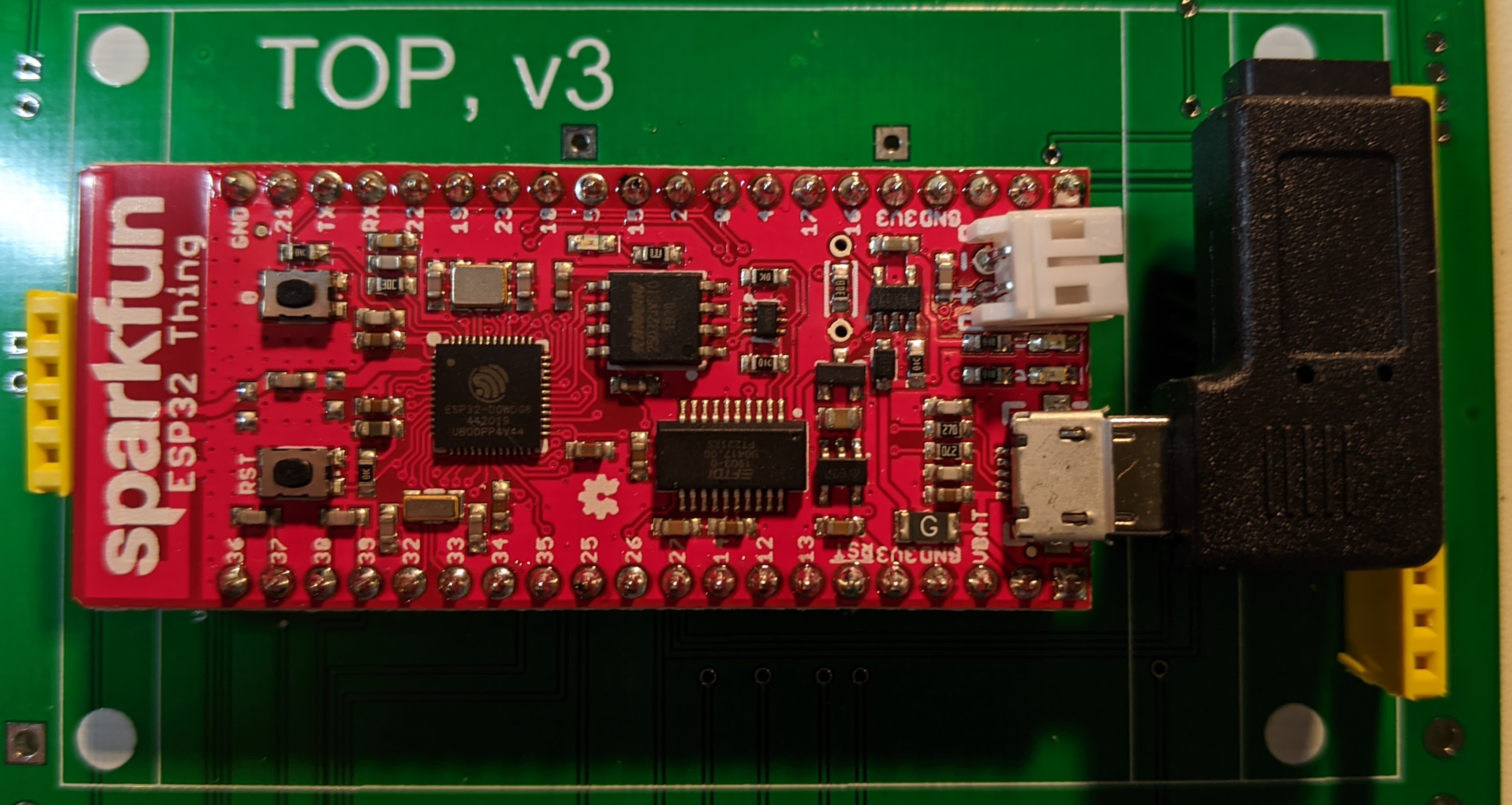
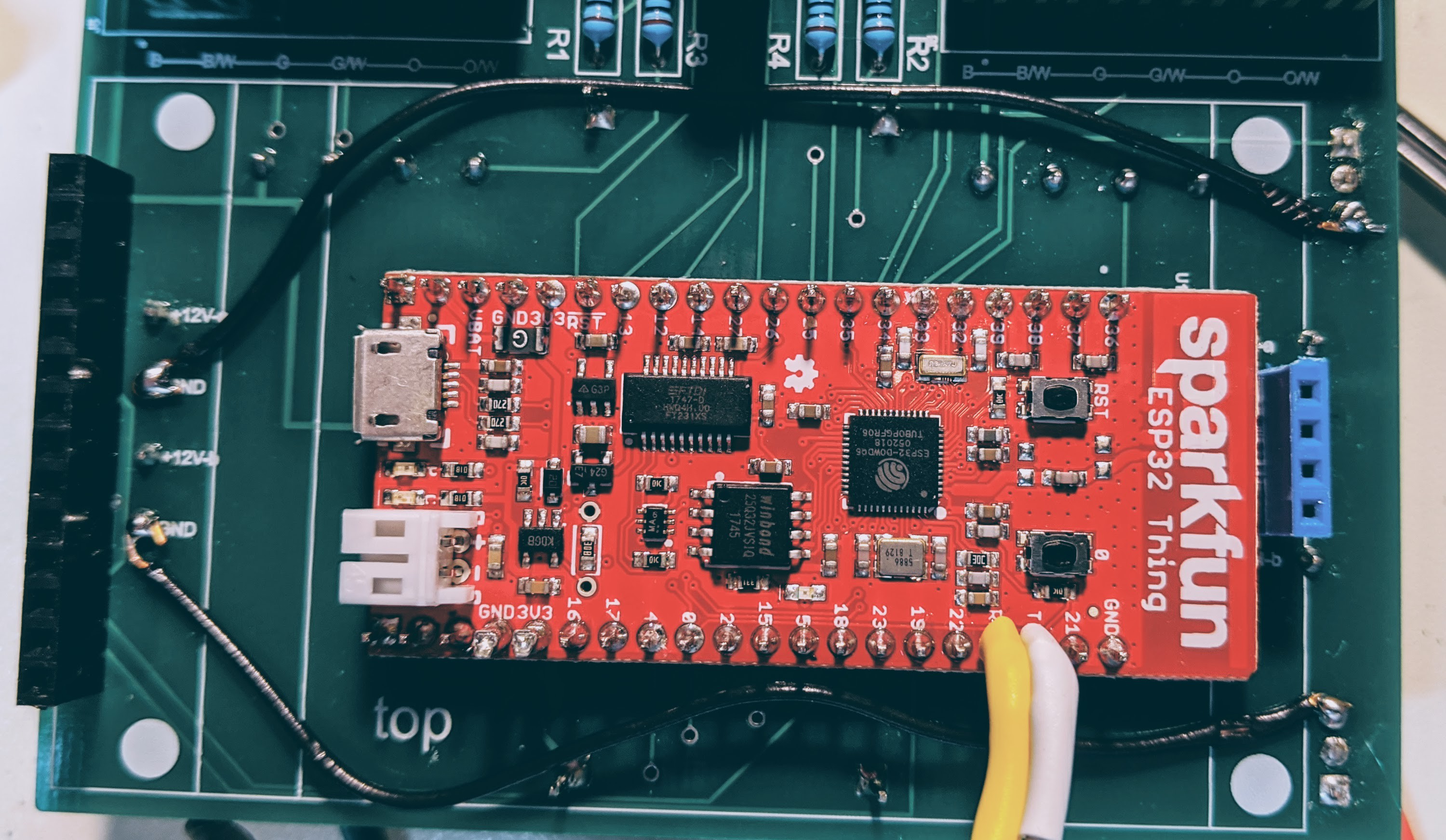
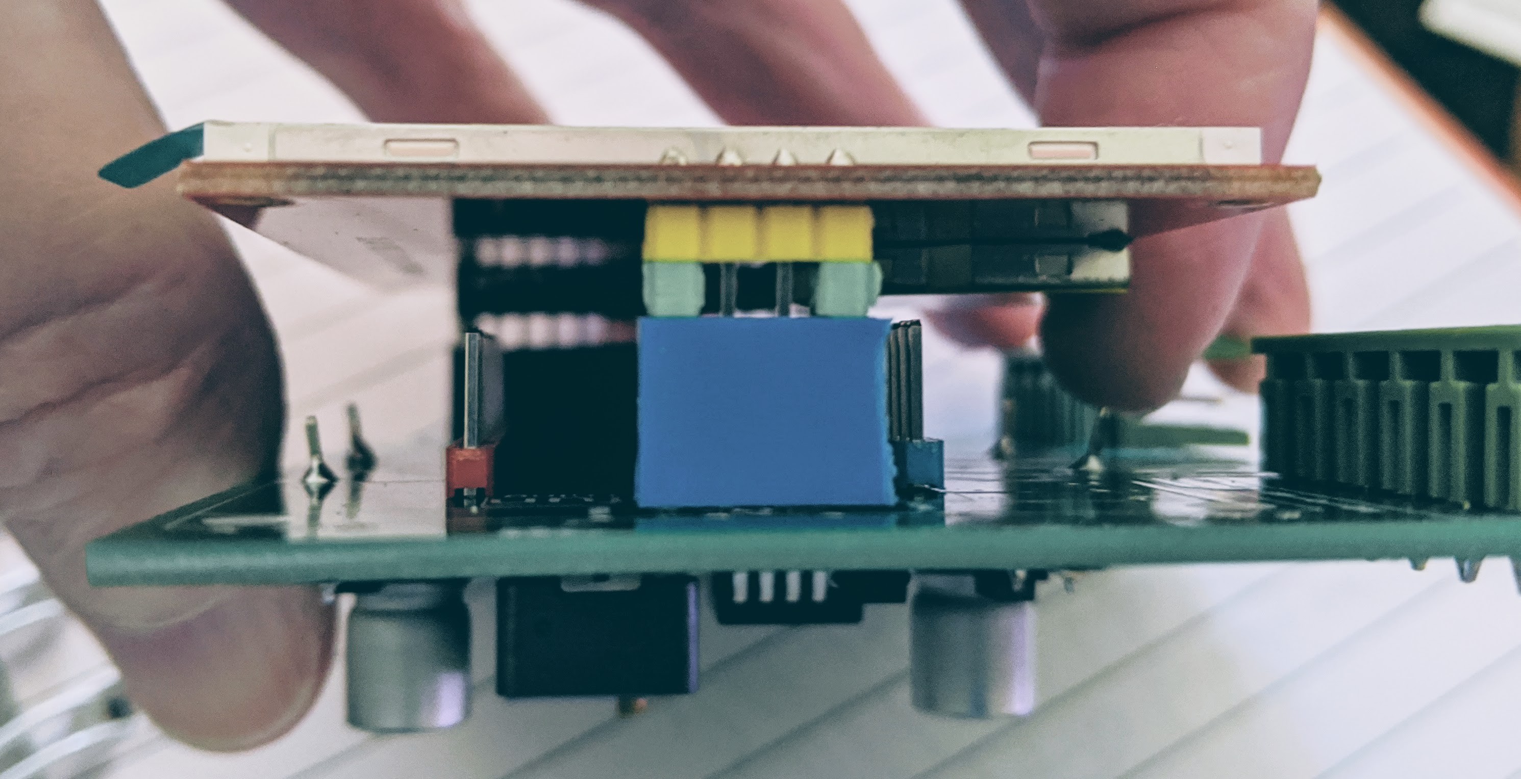
One of the reasons you're struggling to fit this all together is because you're using lots of off-the-shelf components; the power supply is made by someone else, the SparkFun board is made by someone else as is the display. Fitting them all together is always going to be hard in a confined space.

All of these parts are easy to implement yourself - and all of it can be built with a standard soldering iron! Perhaps for your next project, you could try building your own buck converter and use the ESP32-WROOM-32U module instead of a SparkFun ESP32 Thing!

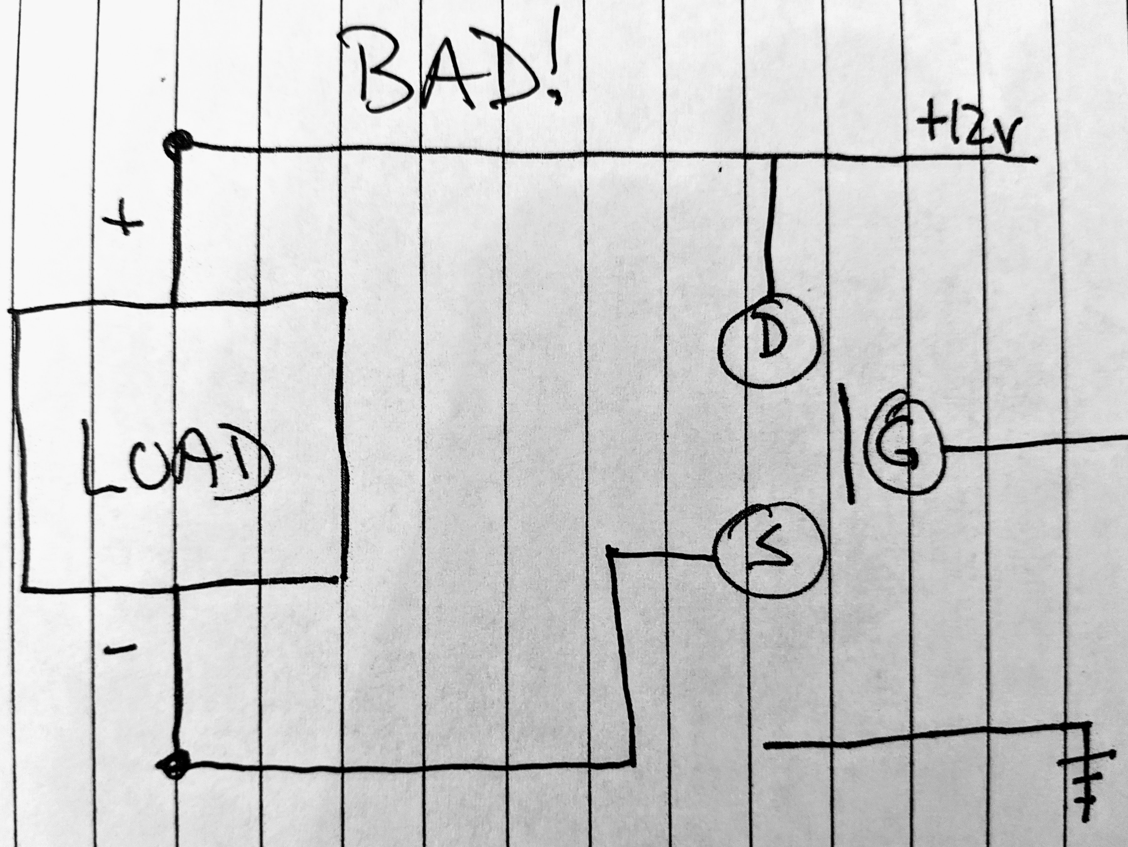
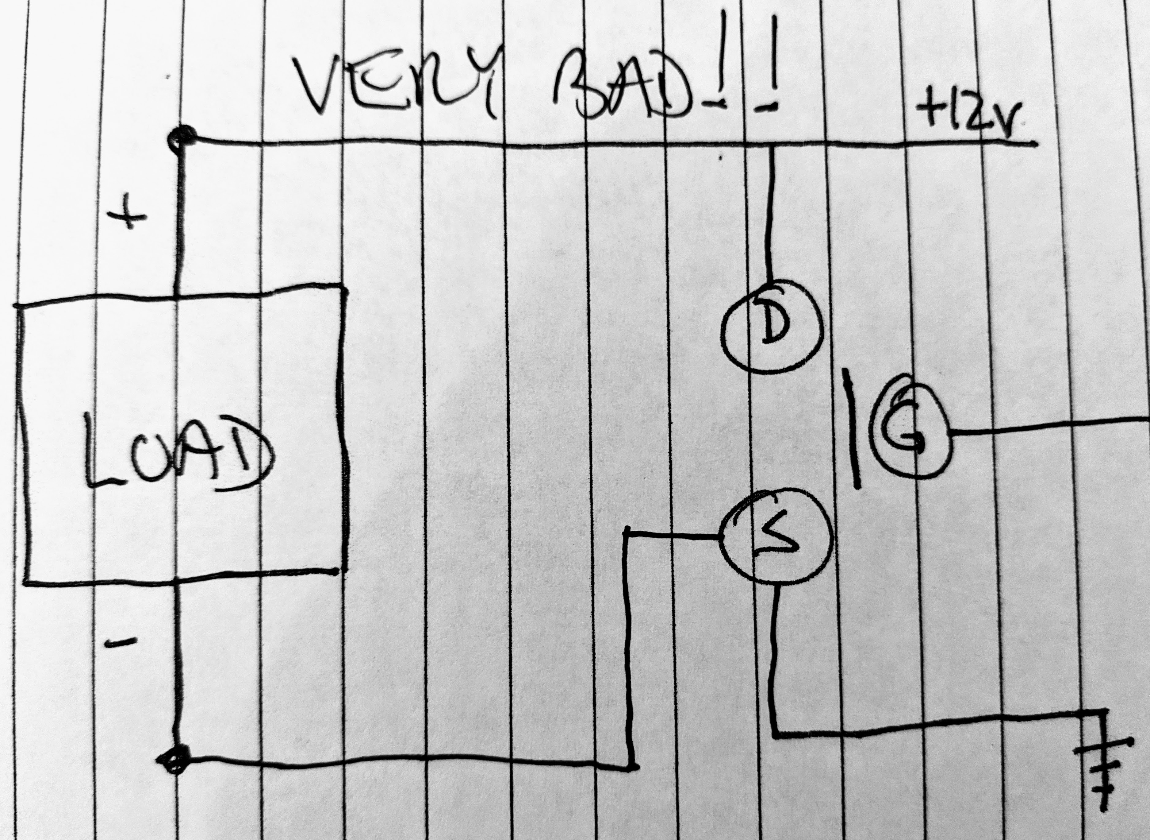
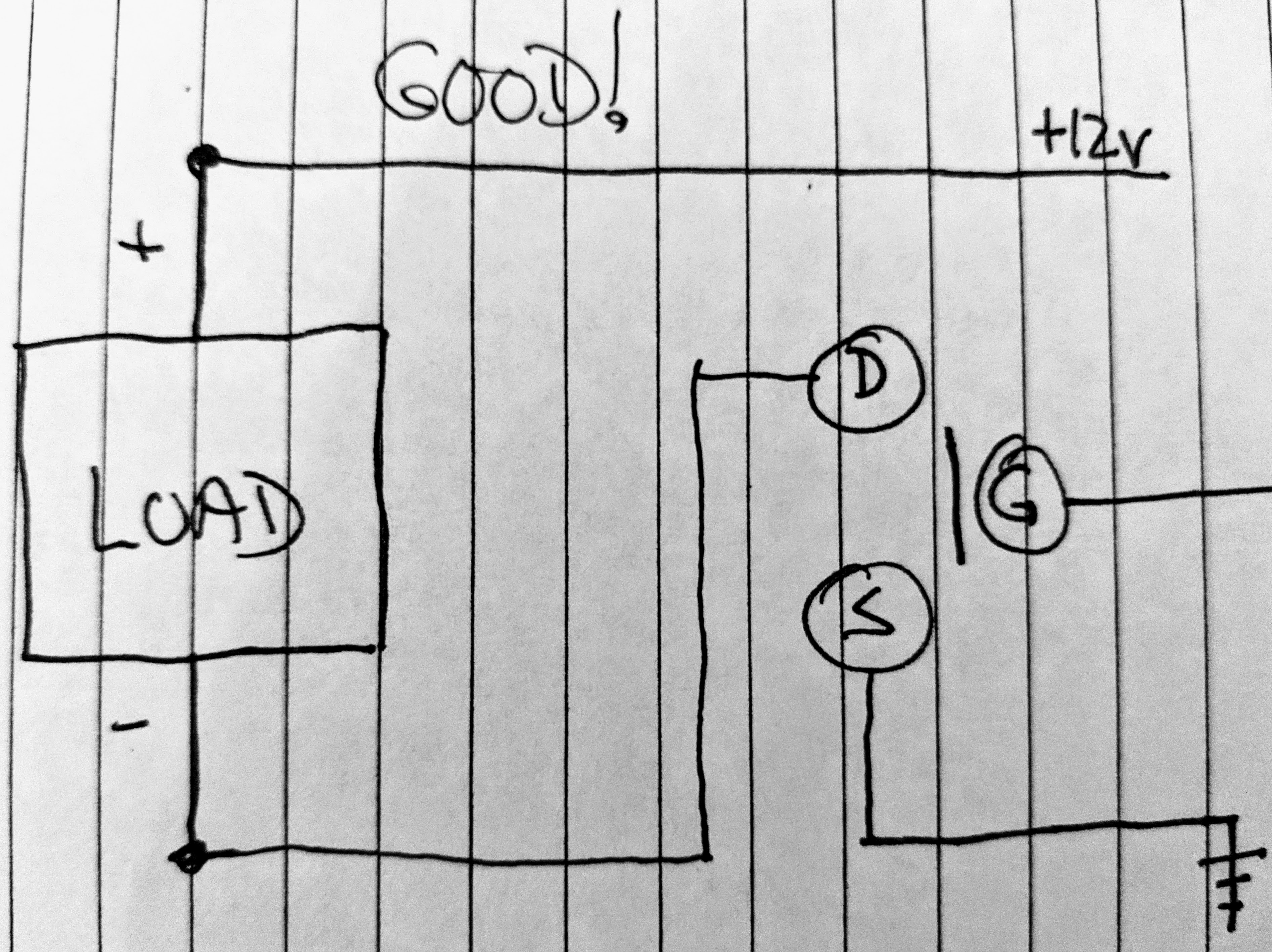
One word of caution - don't connect the USB cable to the SparkFun while you have the main power for the project connected. I can't see your schematics, so I don't know how you've connected things, but it's very likely you'll be connecting two different power sources together somewhere and you could end up damaging either the power supply or the ESP32 Thing.

  Are you sure? yes | no

WJCarpenter wrote 07/02/2021 at 02:00 point

Thanks for your comments. I agree on all points.

I was thinking about finishing this project during lockdown, but something or other happened. :-) 

  Are you sure? yes | no

Graham Toal wrote 07/16/2017 at 02:12 point

This (use a pi zero w for lower cost, or stick with the ESP8266 if you prefer working at a low level) should do most of the analog side for you: https://www.instructables.com/id/Easiest-RGB-LED-Strip-With-Raspberry-Pi/

  Are you sure? yes | no

WJCarpenter wrote 07/16/2017 at 02:30 point

Interesting idea. Thanks.

  Are you sure? yes | no

Similar Projects

Does this project spark your interest?

Become a member to follow this project and never miss any updates