 WJCarpenter
One of the possible mistakes I made in the first iteration of the PCB was in not thinking very precisely about the current capacity of the traces the carry power to the lights. I just laid out the PCB without calculating that. With the larger board area in the V2 PCB, I had room to make those power traces bigger. I wasn't sure how big to make them, so I just SWAGed it at 100 mils.
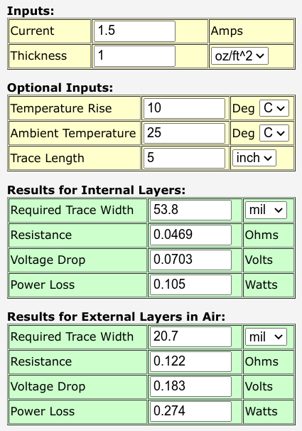
Today, I finally got around to figuring out what I should have done earlier. It's easy to find PCB trace width calculators on the web. I used this one https://www.4pcb.com/trace-width-calculator.html, but there are many others. My earlier measurements were a max of 20w of current draw, less than 1.5A at 12vdc. The PCB is less than 4 inches wide, but allowing for circuitous routing, I used 5 inches.
The calculator tells me I need a trace width of 21 mils for the top or bottom layer. I guess 100 mils should cover it! Even the 50 mil traces that I had blindly used on the V1 PCB now look good enough.
The pins that are connected to the GND copper pour were drawn with wagon wheel connections, which is intended to make soldering easier. I was a little skeptical of the current-carrying capacity of those spokes, so I smudged over some of the gaps with the trace drawing tool to give a thicker connection. Maybe I didn't need to do that, but maybe I'm not an actual EE.
Discussions
Become a Hackaday.io Member
Create an account to leave a comment. Already have an account? Log In.