 WJCarpenter
When I did V2 of the PCB, I wanted to leave more room between the USB connector on the microprocessor board and the tall female headers for the display board. I did that. What I didn't do was pay attention to the other end, the 4-pin female headers for the display board. I faked myself out by relying on the silkscreen image of the Sparkfun ESP32 Thing board. (Which I myself created, so that's my fault, too.) On the silkscreen, it looks like there is plenty of room. On the actual V2 board, that end of the microprocessor board protrudes a few millimeters too far and pushed on the 4-pin header.
I thought I had a good workaround for that. That end of the microprocessor board is fairly empty. It just has a small sliver of empty PCB and then the PCB antenna for wifi. I thought I could carefully shave down that end with a file or some sandpaper. In fact, I still think I can, but it's a tedious and error-prone process. Here's an image generated from Sparkfun's published ".brd" file so you can see what I'm talking about.
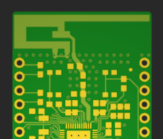
(BTW, that graphic was rendered by Altium's free online viewer (https://www.altium.com/viewer/), which I found to be quite nice.)
After I filed and sanded quite a bit (on a microprocessor board that I had kind of wrecked through earlier foolishness), I was starting to get into the PCB antenna, and it was still pushing on the 4-pin header. I decided that I was becoming part of the brute squad, so I went back to my PCB layout and moved the microprocessor board exactly 100 mils (2.54 mm) "to the east" away from the 4-pin header. The advantage of moving exactly 100 mils is that I could check the spacing on the V2 PCB by just moving the microprocessor board by one pin on the header pins I had placed to check the spacing.
By incredible good luck, it turns out that the microprocessor board with a micro-USB right-angle adapter exactly fits in the space between the two sets of headers for the display board. I don't mean "it sort of fits". I mean, it fits like it was made that way. I'm glad I didn't try to plan it that way, or it would surely have not worked out.
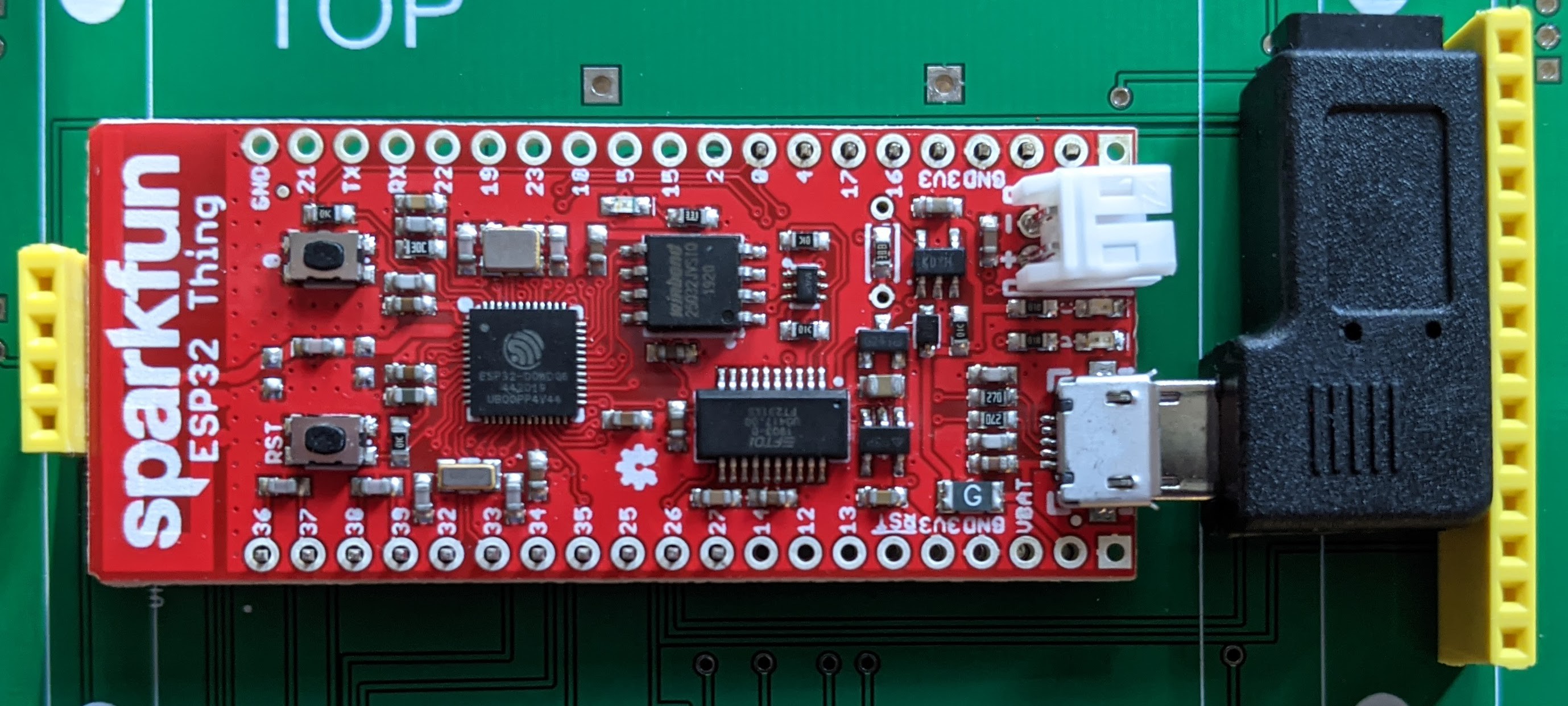
Here's a picture with a microprocessor board that was not filed/sanded at all.
In the upverter.com PCB layout tool, it was easy to move the microprocessor board by 100 mils. I merely had to select the part, hit the "inspect" button, and add 100 to the x coordinate. Re-routing the traces was much more tedious. There might be an easier way to do it, but a lot of things in Upverter aren't completely intuitive to me. It was easy to move vias by the same technique of adding 100 to their x coordinates. For the traces, the only metadata given to me was the trace width and total length. Perhaps I could have done something by exporting to Upverter's "universal" (*cough*) JSON format, editing it, and re-importing it. Instead, I just laboriously moved the traces individually. Man, there sure are a lot of connections coming out of the microprocessor board.
The V3 boards (https://upverter.com/design/wjcarpenter/oelscv3/) are currently being created at jlcpcb.com.
Discussions
Become a Hackaday.io Member
Create an account to leave a comment. Already have an account? Log In.