 agp.cooper
CPU 4
Background.
Weird CPU
My first CPU (https://hackaday.io/project/12879-weird-cpu) was an 8 bit TTA (Transport Triggered Architecture). It has a front panel and sits happily on my shelf chasing LEDs in circles (such is the life of a simple CPU):

Four bit OpCode CPU
My second CPU (https://hackaday.io/project/13017-4-bit-ttl-cpu) was a 4 bit OpCode CPU. A bit of a disaster, I decided to get PCBs made rather than use strip-board. After 5 revisions (i.e. PCBs) I still do not have it working. I just do not know how many more PCB revisions I will need to get it working.
Subleq CPU
My third CPU design was a Subleq CPU (https://hackaday.io/project/25133-a-subleq-cpu). I quickly realised that it was too inefficient to fit into 8 bits so I moved to 16 bit. This meant I could not use a front panel for programming (i.e. a few hundred bytes is okay but a few thousand words is not!). The decoder started to get complicated as I had to add direct memory access for the programmer (i.e. an Arduino).
Subleq is also very cryptic. So I ported a simple compiler (https://hackaday.io/project/25583-simple-compiler) to export Subleq and wrote a Subleq assembler and interpreter for simulation.
This project too was abandoned as it had migrated so far from an interesting curio to a programming monster. I did learn a lot about compilers and what is expected from the CPU.
CPU 4 Details
CPU 4 is a complete rethink about my home brew CPUs:
- I need to use OpCodes for programming efficiency.
- I need to radically simplify the OpCode decoding logic.
The usual approach is to use a ROM or a PLA to decode the OpCodes. I have not adopted this approach because I would like to option to convert the design into DTL (i.e. build a transistor CPU).
TTA CPU
I did look at the possibility of using my TTA CPU to interpret OpCodes. It is possible but not well suited for the task. However, if the TTA CPU does not need to access RAM directly then the decoder logic is greatly simplified.
A structure like [DST][SRC] could be used where [DST] is a register and [SRC] is a register.
TD4
TD4 uses this OpCode approach to a degree (https://hackaday.io/project/8442-ttl-based-4-bit-cpu). TD4 also has access to immediate data (which is why it is so interesting) but the approach for immediate data is very primitive. Every OpCode has immediate data attached to it (very inefficient). So adding immediate data on demand would be very useful.
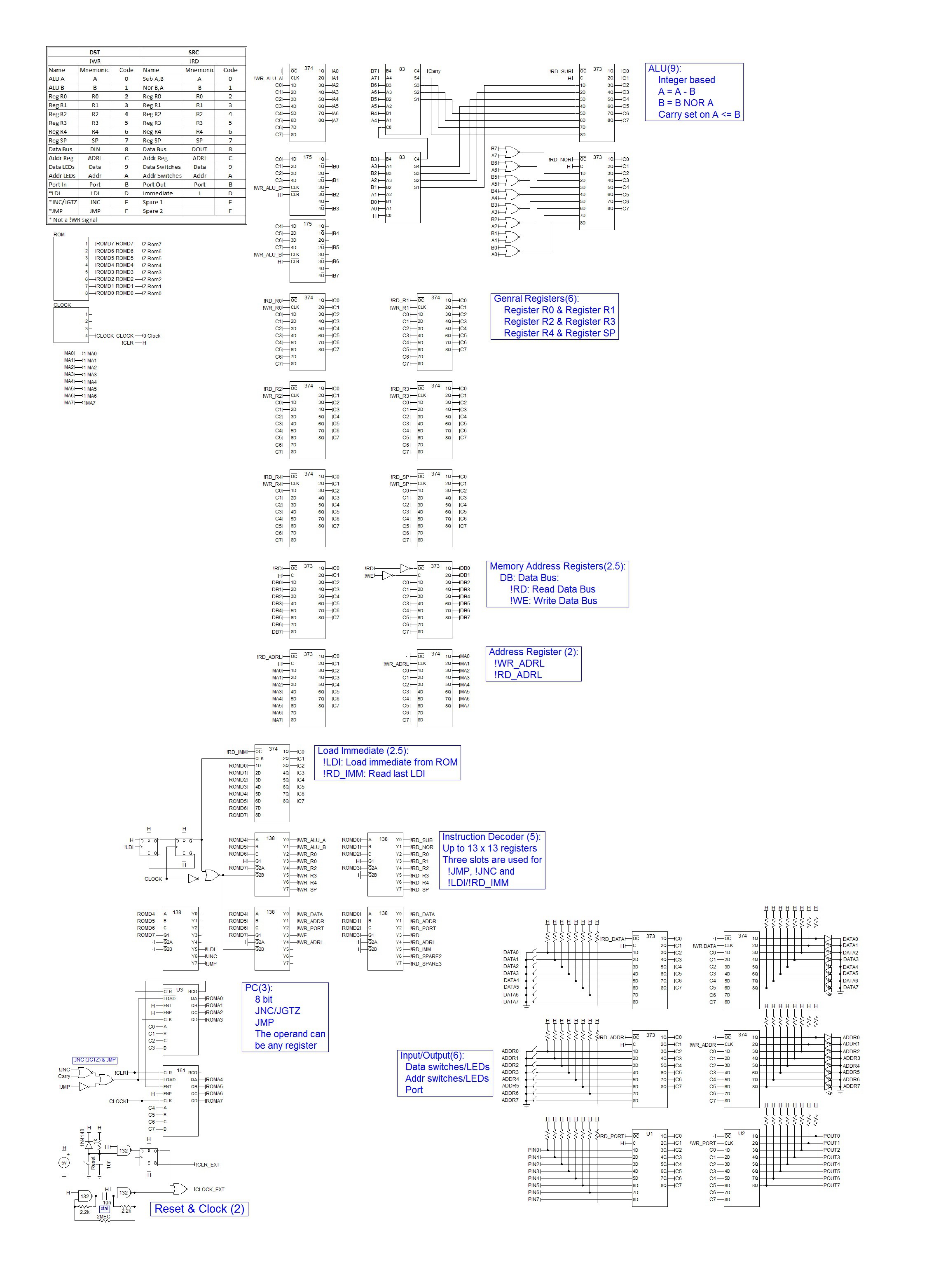
The Decoder
Here is the schematic for the decoder:
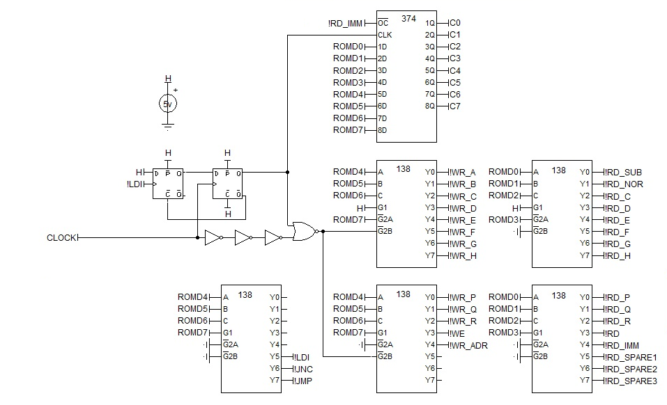
So what you will notice is that I have used 74LS138s to decode the OpCode [DST][SRC].
[DST] is 4 bits (16 options) and [SRC] is 4 bits (16 options). A [DST] is actually a clocked signal while the [SRC] is an out put enable signal. The exception is the three [DST] that are not clocked !LDI (load immediate), JNC (jump on not carry) and JMP (unconditional jump). Very simple is it not!
The !LDI logic blocks the write clock to all the registers (but not the program counter) and instead clocks the 74LS374 latch. This catches the next ROM address as immediate data (if the [DST] decodes to !LDI).
From the schamtic you should be able to see that the CPU can have up to 13 write registers and 16 read registers.
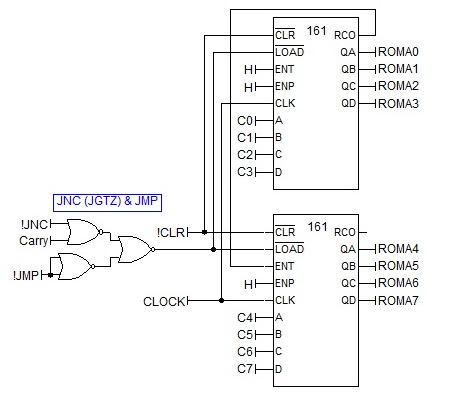
The Program Counter
The program counter is pretty straight forward:
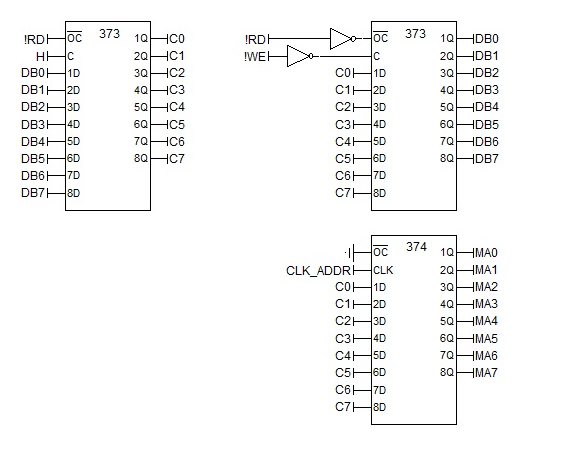
The External Data Bus
For the CPU to access RAM (i.e the user program), the general registers need to configured as read/write:
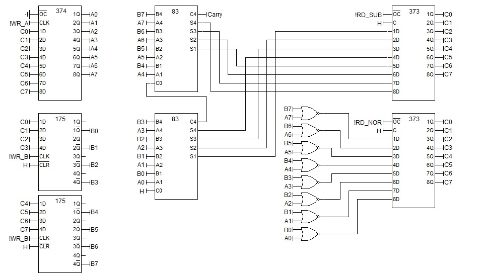
The ALU
The ALU is similar to the Weird CPU but I use integers, subtraction and NOR instead:
The OpCodes
So here are the OpCodes (these have been updated since my initial post):
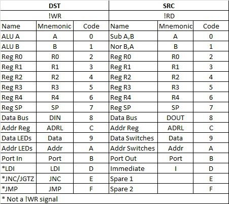
The OpCodes are constructed as [DST][SRC]. So "mov A, B" would be coded as 0x01.
LDI is different as its source is the ROM so the [SRC] and be anything.
Another example is to increment the C Register:
- LDI
- 0xFF ; -1
- B, I ; Short for mov B, Imm
- A, R0 ; Load A with R0
- R0, A ; Set R0 with A - B which is the same as A + 1
The above code takes 5 cycle cycles. The Weird CPU (TTA) would take 12 cycles. My Subleq CPU would take 36 cycles.
Reading and Writing to Memory (RAM)
Reading and writing to RAM, lets us increment memory at address C:
- LDI
- 0XFF
- B, I
- ADRL, B
- A, DIN
- DOUT, A
Six clock cycles, not bad.
The Design Concept
Here is an early CPU 4 design concept (mainly the register names have changed):

The Schematic
And finally the full schematic:
AlanX