 kodera2t
If we see "commercial standard" of HDL writing environment among FPGA/CPLD providers, we are so happy but unfortunately their programming interface is completely different for company by company. Comparing the case of Xilinx ISE and Lattice Diamond, we still see different experience. Here I would like to show how to write HDL on this board step by step.
Before starting, we need to download Lattice diamond and get free license. After installing diamond, yeah let's get started!
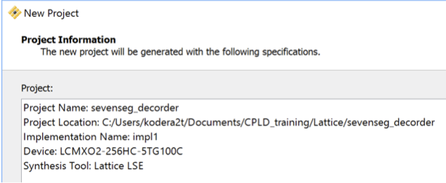
Step 1: Make new project
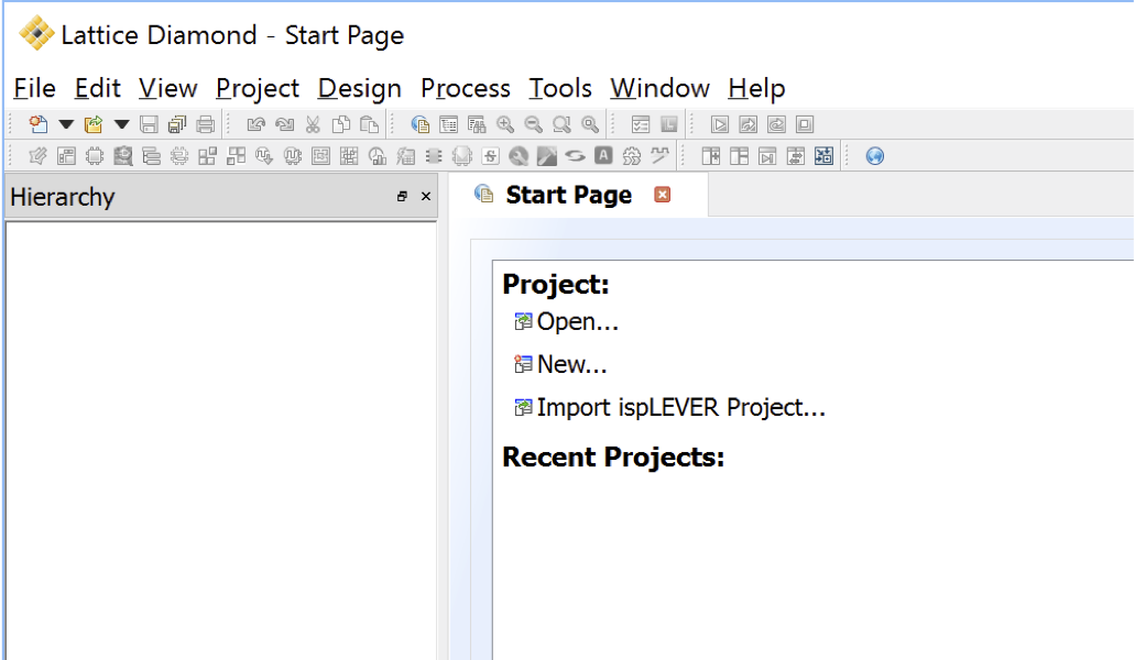
Selecting proper (32bit or 64bit) version of Diamond, just click will show you start page.
Let's click "New..." and make and name new project
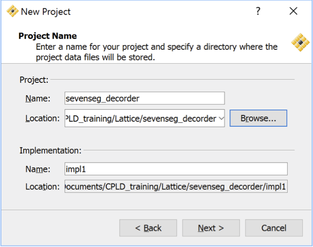
The default location is not good one and we can switch to user directory and name project name as we wish and click next..
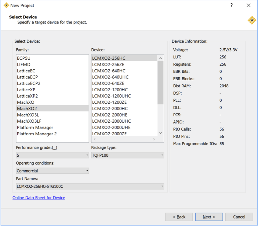
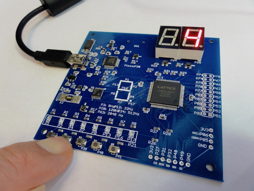
We need to select device here. The board has
LCMXO2-256HC-4TG100C
which has TQFP100 package and 256LUT. Let's select this device and click next..
Now it will show you project summary. Here let's add Verilog file!
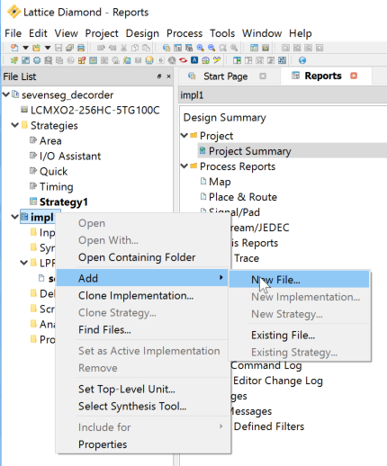
Step 2: Write your file!
On "impl", right click and add "New File" will show you the following...
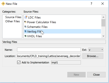
If you prefer VHDL, just select VHDL files for source files but the example here will be done by Verilog Files. Put name of verilog file (I named "sevenseg.v" ) and click "New" then editor window will appear.
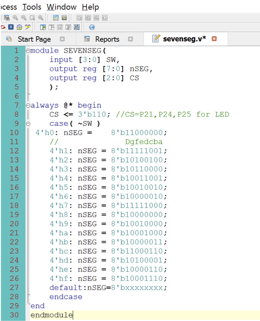
Any Verilog file are ok but let's write sample like above. This is seven segment decorder. Please note that, this board is "negative logic", means "active low". The Lattice Diamond will check your code in real time and if something is wrong, you will see some error message at the bottom of window.
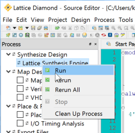
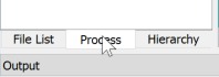
After writing, let's synthesize by right-click "Lattice Synthesis Engine". Switching file list and Process list, just click process tab as below..
Step3: Let's connect HDL and real world!
If no error, we can proceed to programmer section. At this moment, we don't have .ucf in Xilinx manner and we need to define pin connection of implementation.
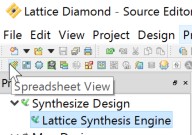
Click "Spreadsheet View" will show you spread sheet of connection.
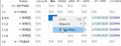
Now let's connect SW[0] to P48 by right click Pin column and select "Assign Pins..."
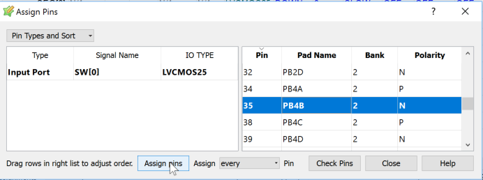
In the right side, we can select Pin and select P48..
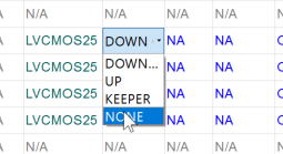
On the board, all interfaces are correctly pull-up or pull-down so please select "NONE" for PULLMODE.
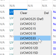
This board is ruining at 3.3 V so please select "LVCMOS33" for IO TYPE
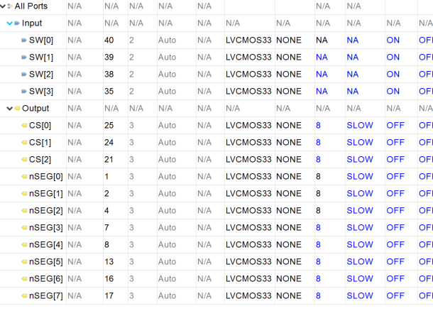
The above picture shows the completed setting. Setting has more options but at this moment we don't need to touch (and I need to explore...)
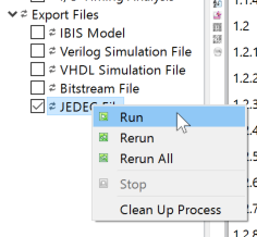
Now let's prepare the implementation. Check "JEDEC File" export and right click will make files to be uploaded to the board.
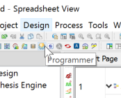
Step 4: Let's program your board!
If no error as above, let's click "Programmer" button as below,
This click will show you the next window,
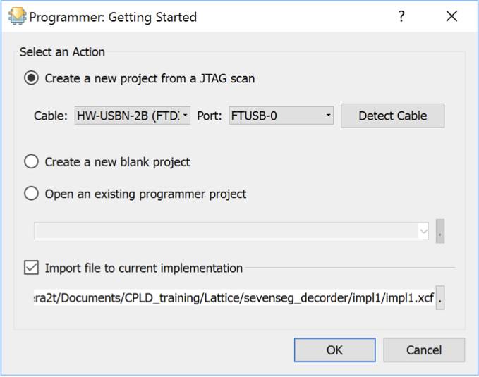
If not selected FTDI as cable, please select "HW-USBN-2B" or similar type with FTDI interface. After selecting proper "cable" let's click OK..
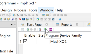
Now the environment will already recognize the board device. Let's click "Program" button. It will find your board and upload implementation to the board and you will see seven segment decorder!
Welcome to software described circuit world!
Discussions
Become a Hackaday.io Member
Create an account to leave a comment. Already have an account? Log In.