 Roger Curry
The selection of letters from SWAN auditory scanning can be accomplished using the phone's own sensor inputs (i.e. the touch screen, accelerometer or proximity sensor). However, using them may be impossible because of insufficient feedback, or a user's lack of dexterity. It's highly desirable therefore, that an external switch, specifically designed for use by the disabled, can be used with SWAN via a 3.5mm jack socket.
These are called AAC switches, examples can be seen here -

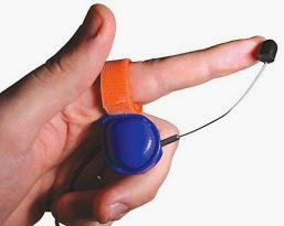


Augmentative and alternative communication switches
more can be found here
To interface these switches to the android smartphone, electromagnetic coupling will be used (details here). A microswitch, for example, can be connected to a coil of wire and a battery via a resistor to limit the current to around 60mA. The coil is placed on the phone, when the switch is closed a magnetic field is generated by the coil, and is detected by the geomagnetic sensor on the phone.
Proof of concept -
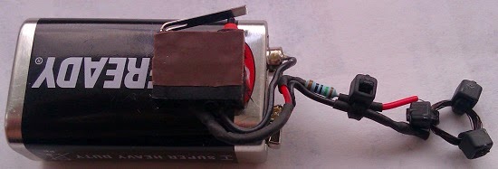
9 V battery, microswitch, 150 ohm resistor, coil of 30 turns of 46 SWG wire, cable ties.
Instead of the microswitch, any commercial AAC switch could be incorporated into this interface via a 3.5mm jack socket.
The simplicity of this means that those of a hacking nature should be able to make such an interface with little effort, from materials at hand, or from a scrapyard or dump. I plan to produce a video showing how quick and easy such a build is, with only parts gleaned from a scrap car.
However, a properly designed interface is desirable, for those able to afford it. To this end I've been learning how to use Eagle PCB software. Years ago, I earned a living using acetate sheets, transfers, black tape of various widths and a scalpel. Now, using CAD is wonderful, compared to the "olden days" of tape up. Here's where I'm at with the design of a double sided PCB to (hopefully, if it works - i.e. produces sufficient magnetic field) replace the coil of wire...

One inch coil, 42 turns of 0.01 inch trace. The vertical lines are screen faults on my "weathered" laptop
The PCB will be populated with -
a wound coil (if the copper trace coil doesn't work)
current limiting resistor
>70mAH li-ion battery
MCP73831 or MAX1555 charge management IC (with associated caps)
charge LED
micro USB socket
test push button
3.5mm mono jack socket
In order that the magnetic interface can be used for purposes other than AAC, pads and traces will be on the board for optional components (a transistor & resistors) and connections (to a PIR device for example, see here).
Discussions
Become a Hackaday.io Member
Create an account to leave a comment. Already have an account? Log In.