 agp.cooper
One Bit CPUs
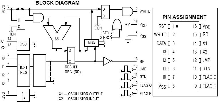
There are a couple of one bit CPUs on the Internet. I have start with the MC14500B chip. This chip was used many years ago for PLCs but the documentation is still available:
http://tinymicros.com/mediawiki/images/e/ec/MC14500B_Handbook.pdf
and
http://tinymicros.com/mediawiki/images/6/65/MC14500B.pdf
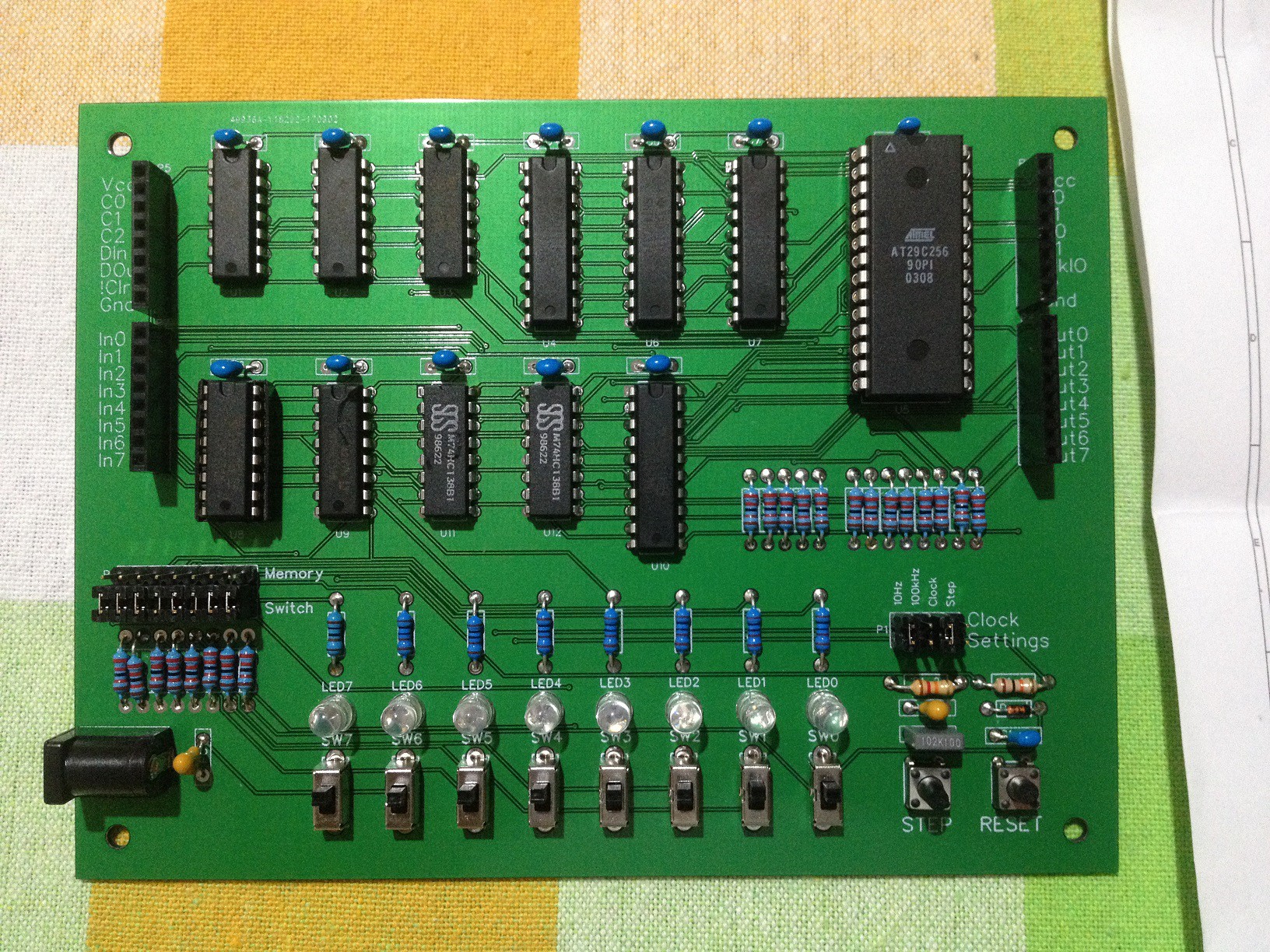
I bought a couple of chips from ebay in case I decide to build a system.
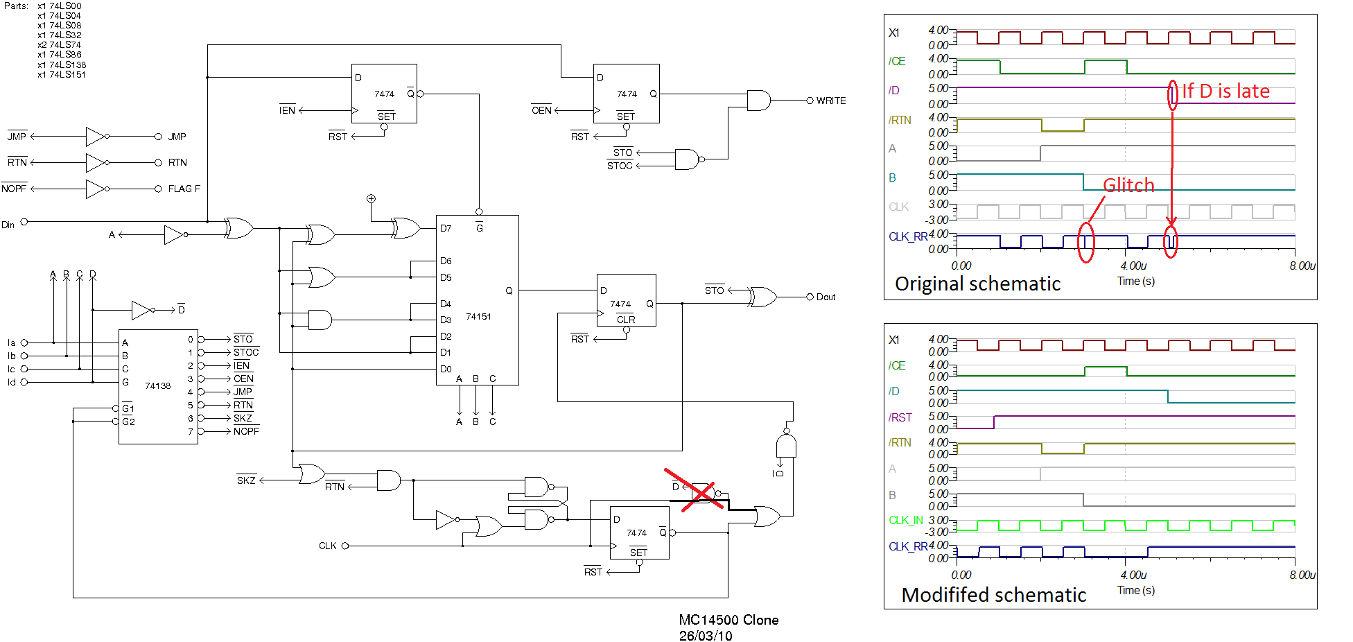
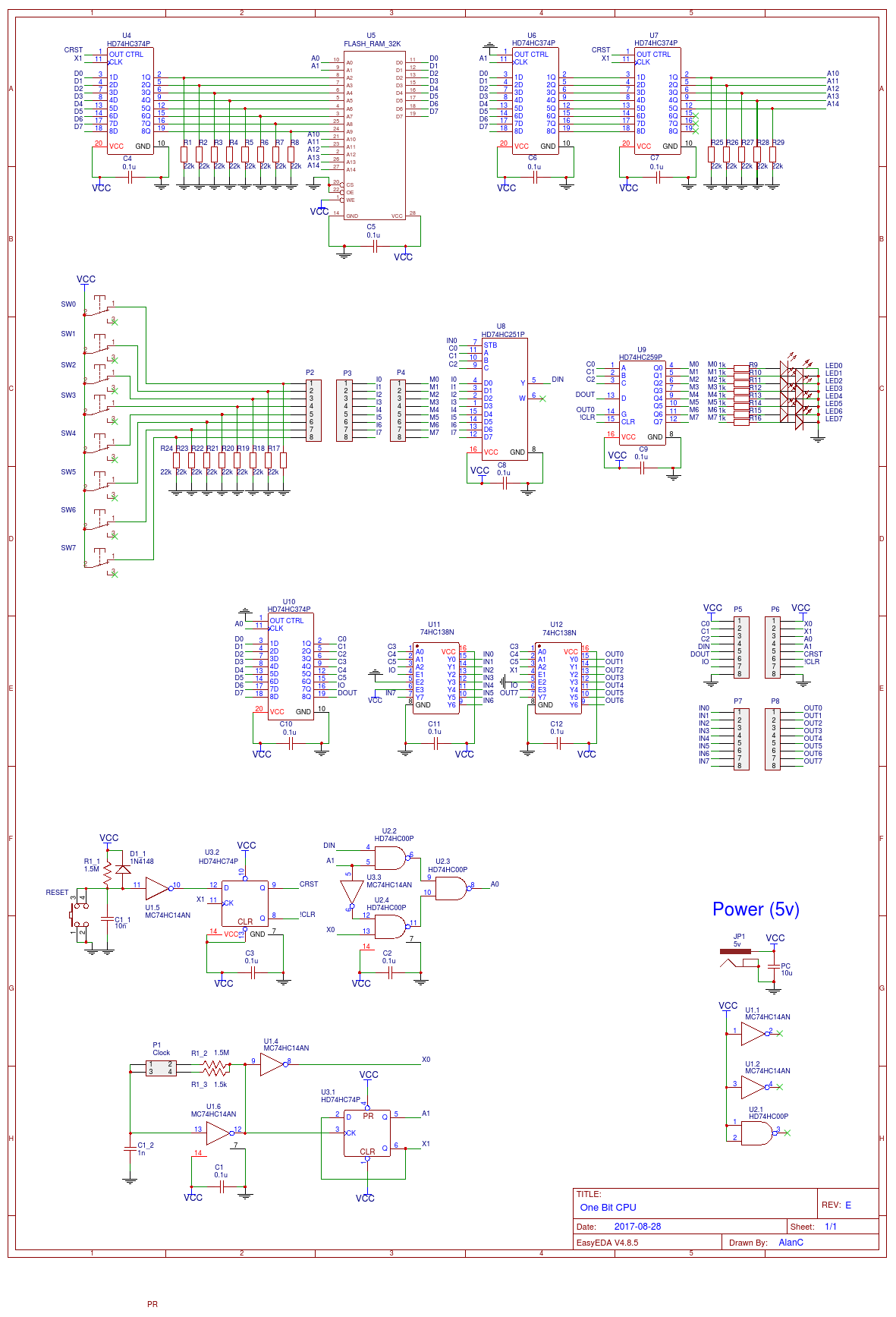
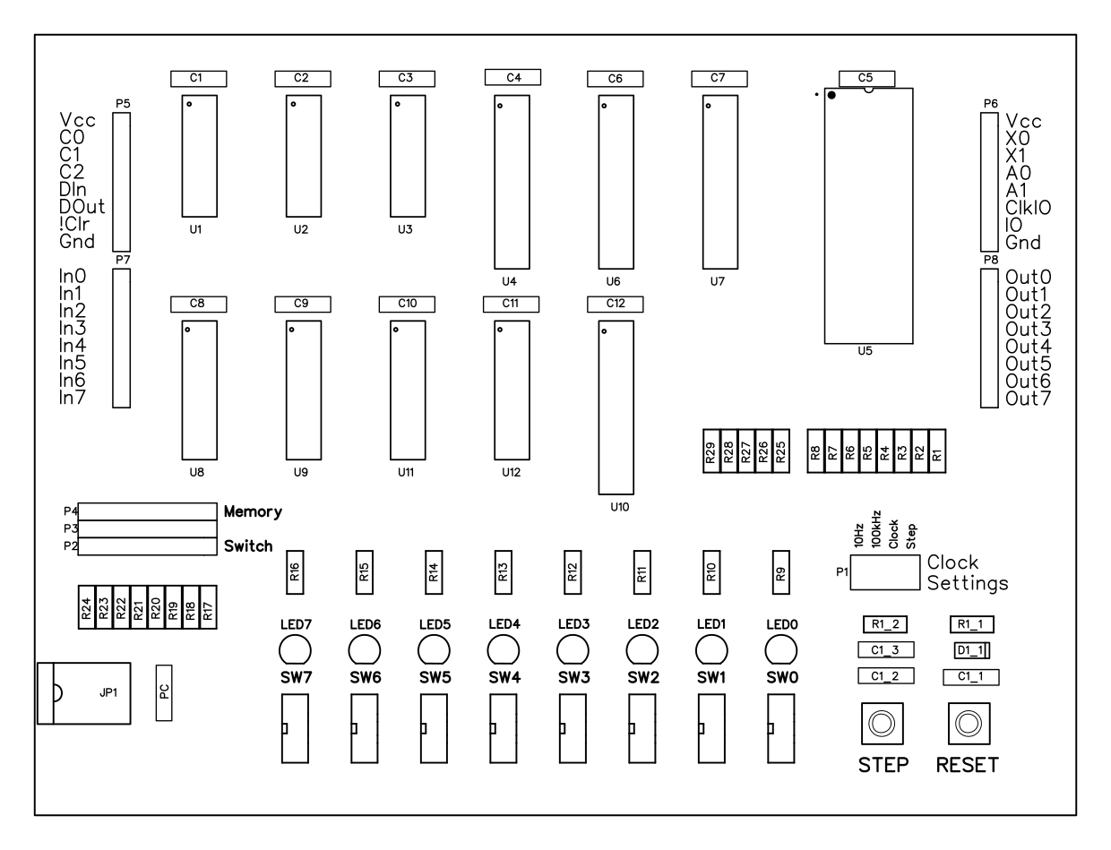
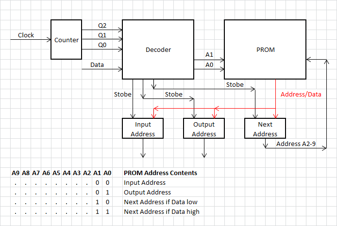
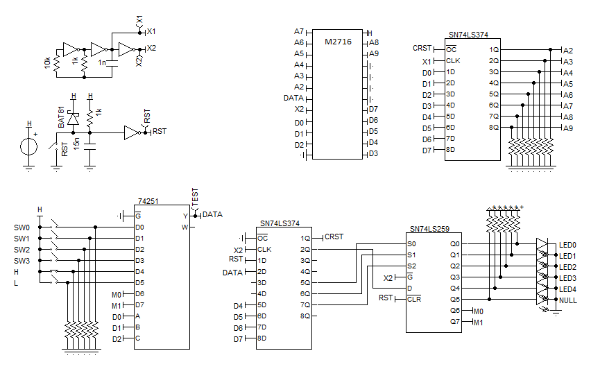
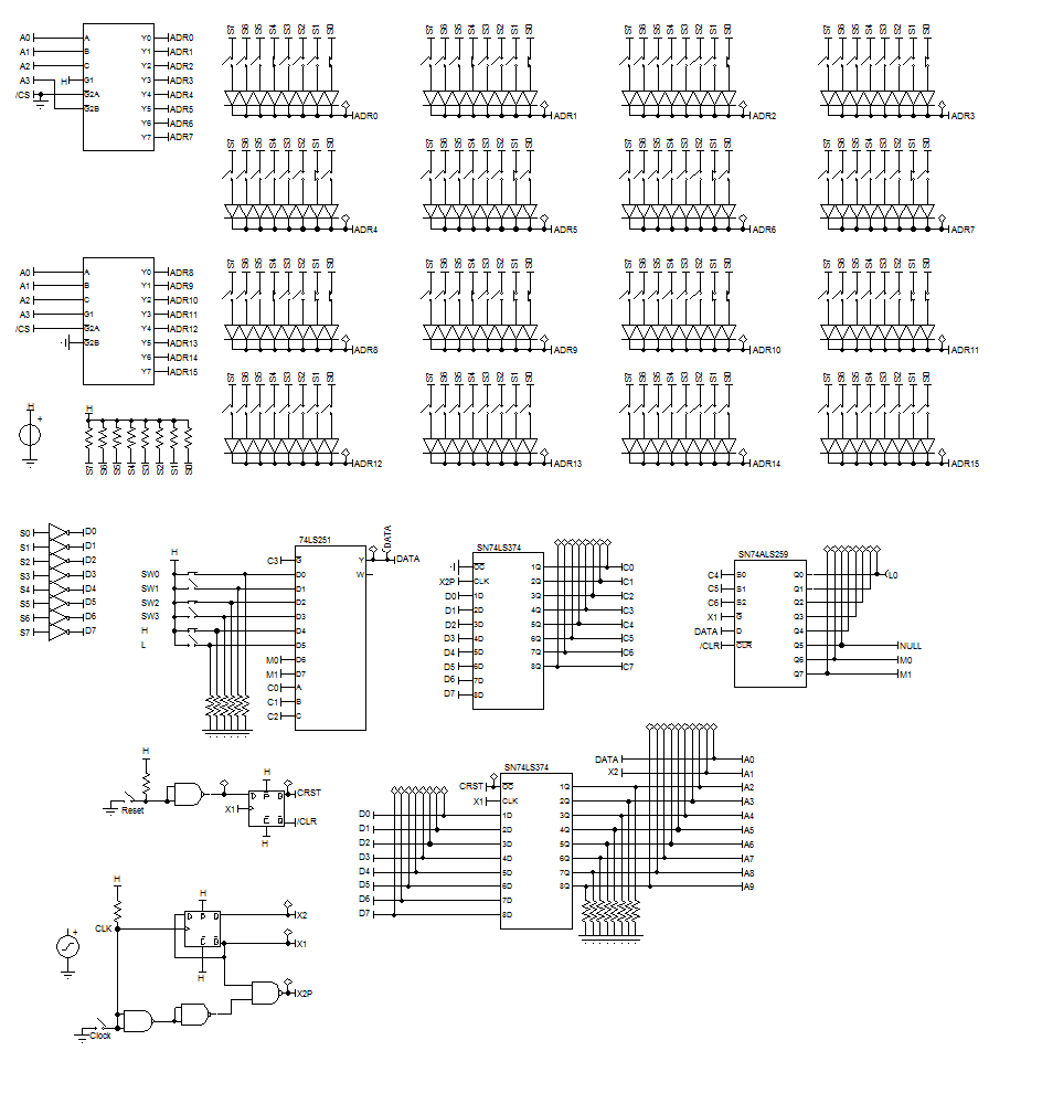
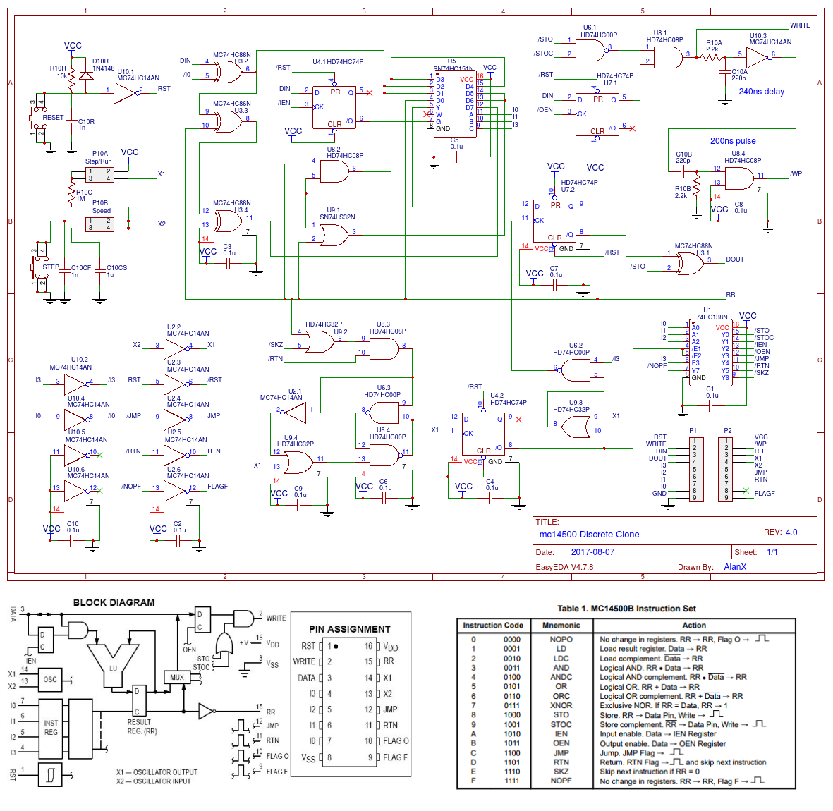
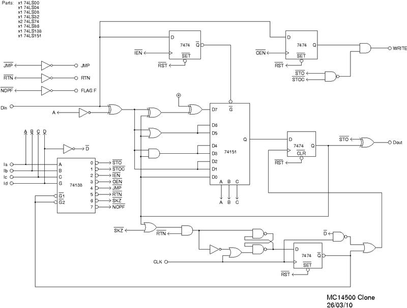
This guy (name unknown) built a clone from discrete chips:
I got the schematic from the Wayback Machine:

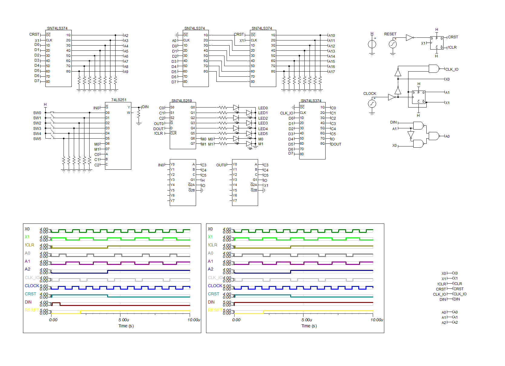
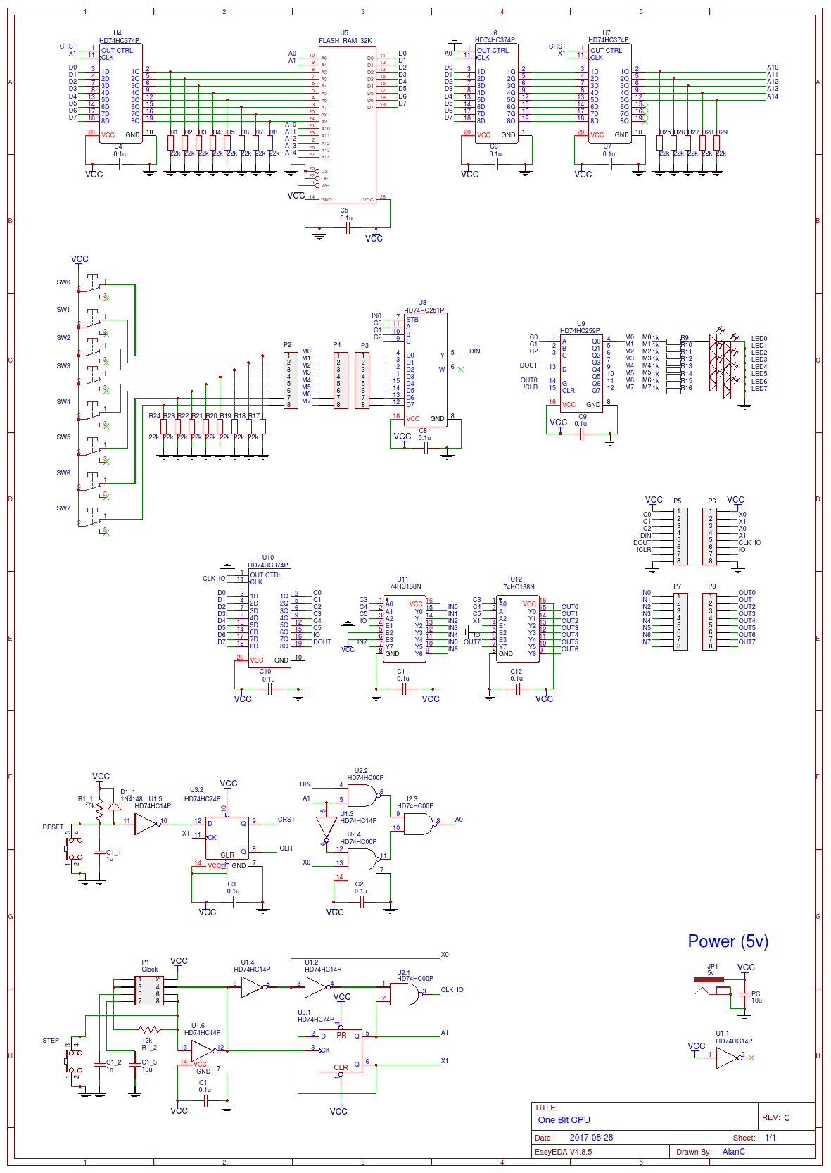
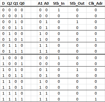
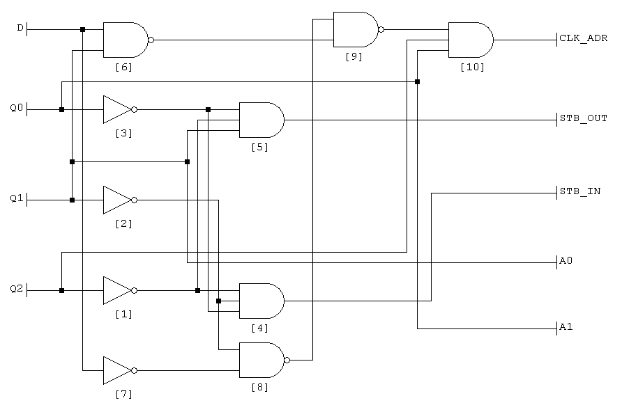
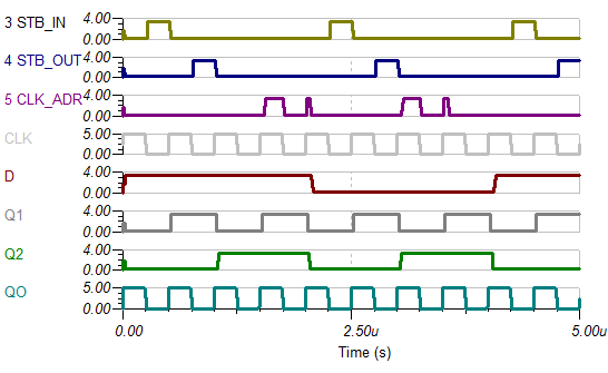
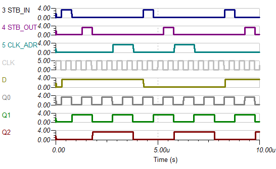
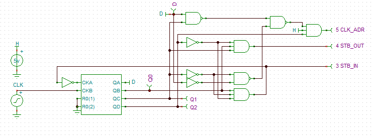
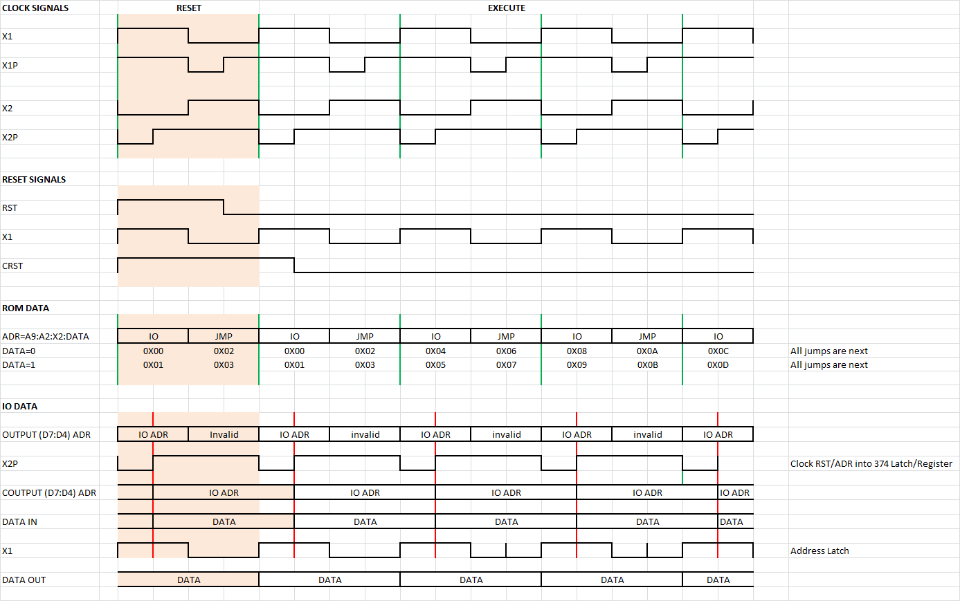
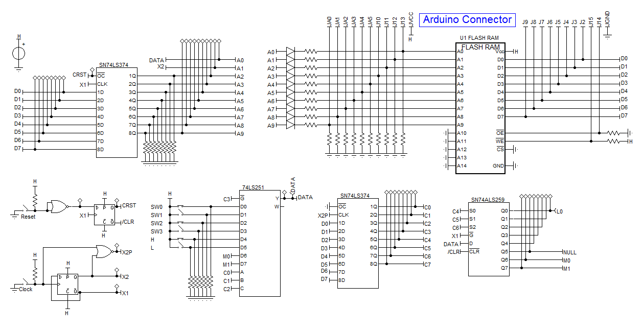
Now I think the RR clock logic is flawed so here is my edited version:
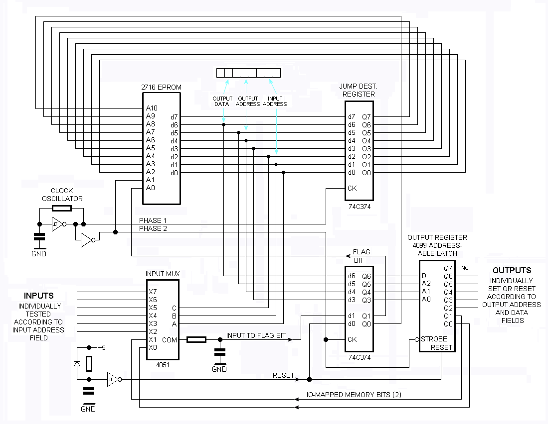
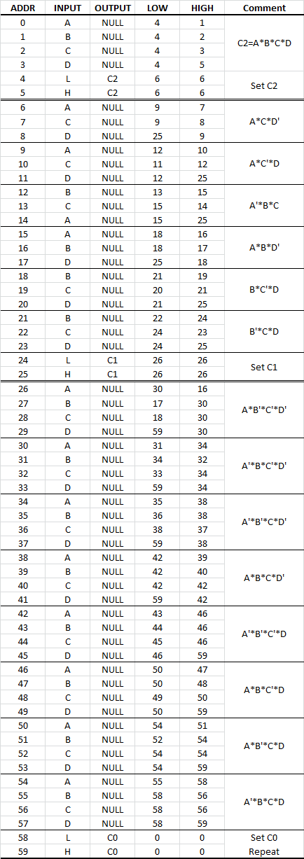
The other one bit CPU that caught my eye was from Laughton Electronics:
 Source:
http://laughtonelectronics.com/Arcana/One-bit%20computer/One-bit%20computer.html
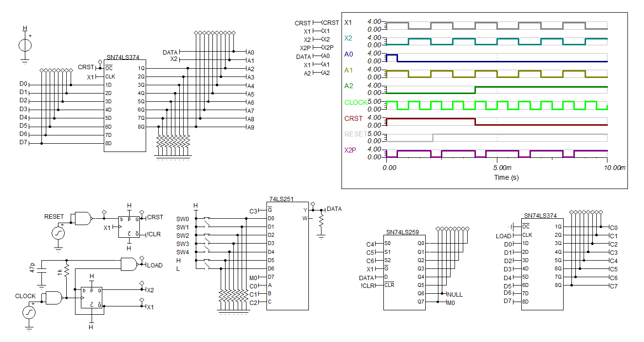
I thought of this machine as a Finite State Machine (FSM), which could be difficult to program (binary FSM can get very complicated very quickly)), but upon sleeping on it, it does not seem that bad. Still, I suspect this machine does not make sense to most people!
There are other one bit CPUs but these two seem to be the best.
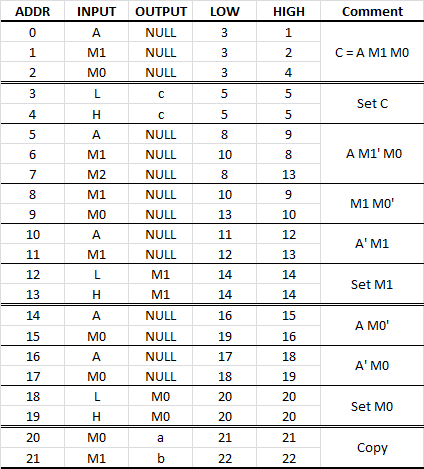
How do they work? They only have 1 bit!
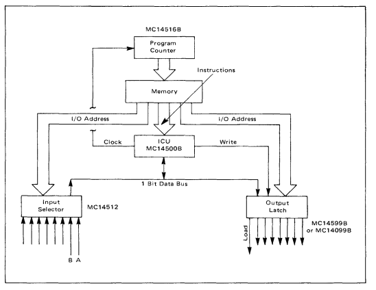
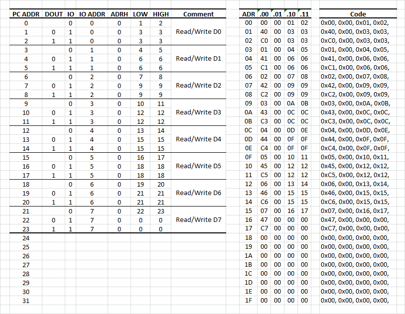
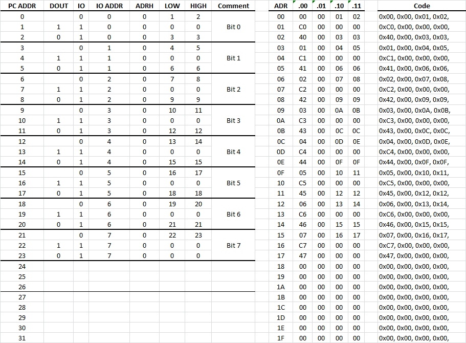
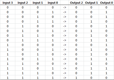
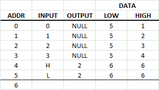
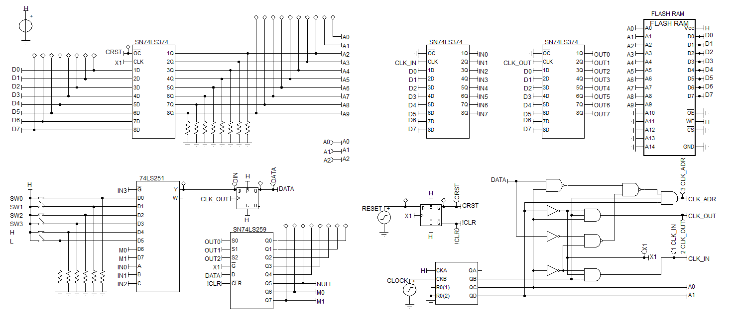
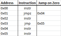
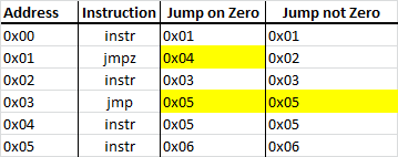
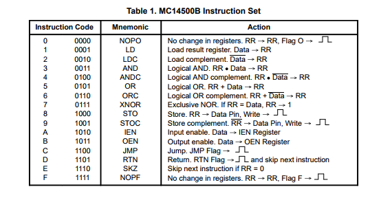
A basic one bit CPU will have an input port(s) and an output port(s). It will read the input port a bit at a time, process the bit (using stored data about previous bit reads) and write to the output port. The example below reads A and B and if both are high then turn on the Load (i.e. Load = NOT(A) AND B):
Here is the code:
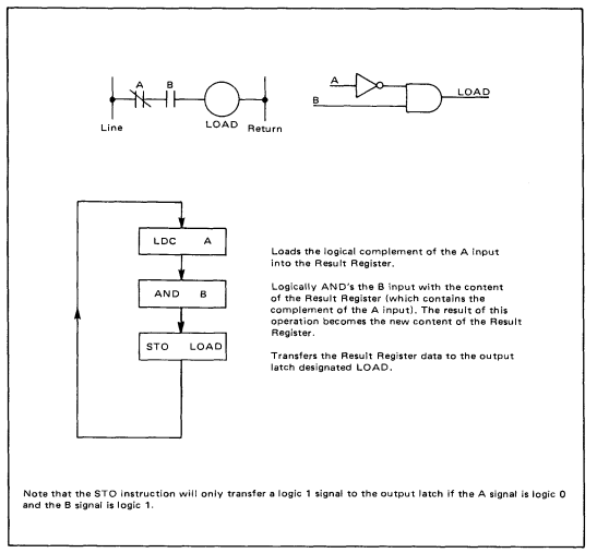
(source: http://tinymicros.com/mediawiki/images/e/ec/MC14500B_Handbook.pdf)
So providing you only want to use logic to control something, one bit CPUs will work quite well (e.g. think of a set of traffic lights).
But, not that fast and not very efficient at doing any mathematics.
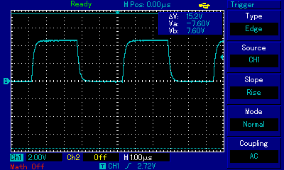
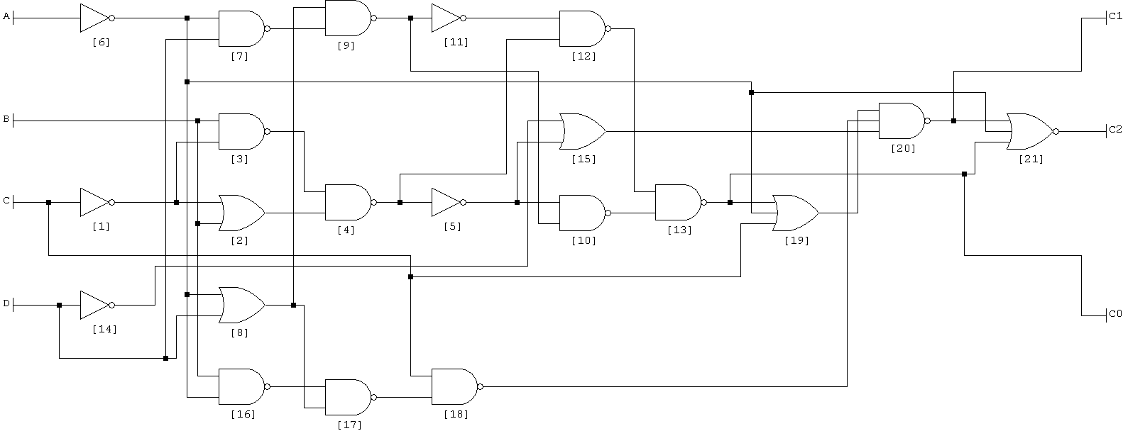
 (Note: The NAND gates are schmit triggers)


 Anders Dinsen
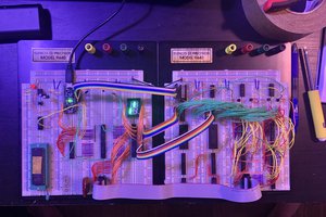
 Tim Ryan
 Tom
Tom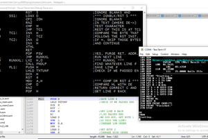
 zpekic
Hi Rue, yeah I am still here but rather busy renovating my house.
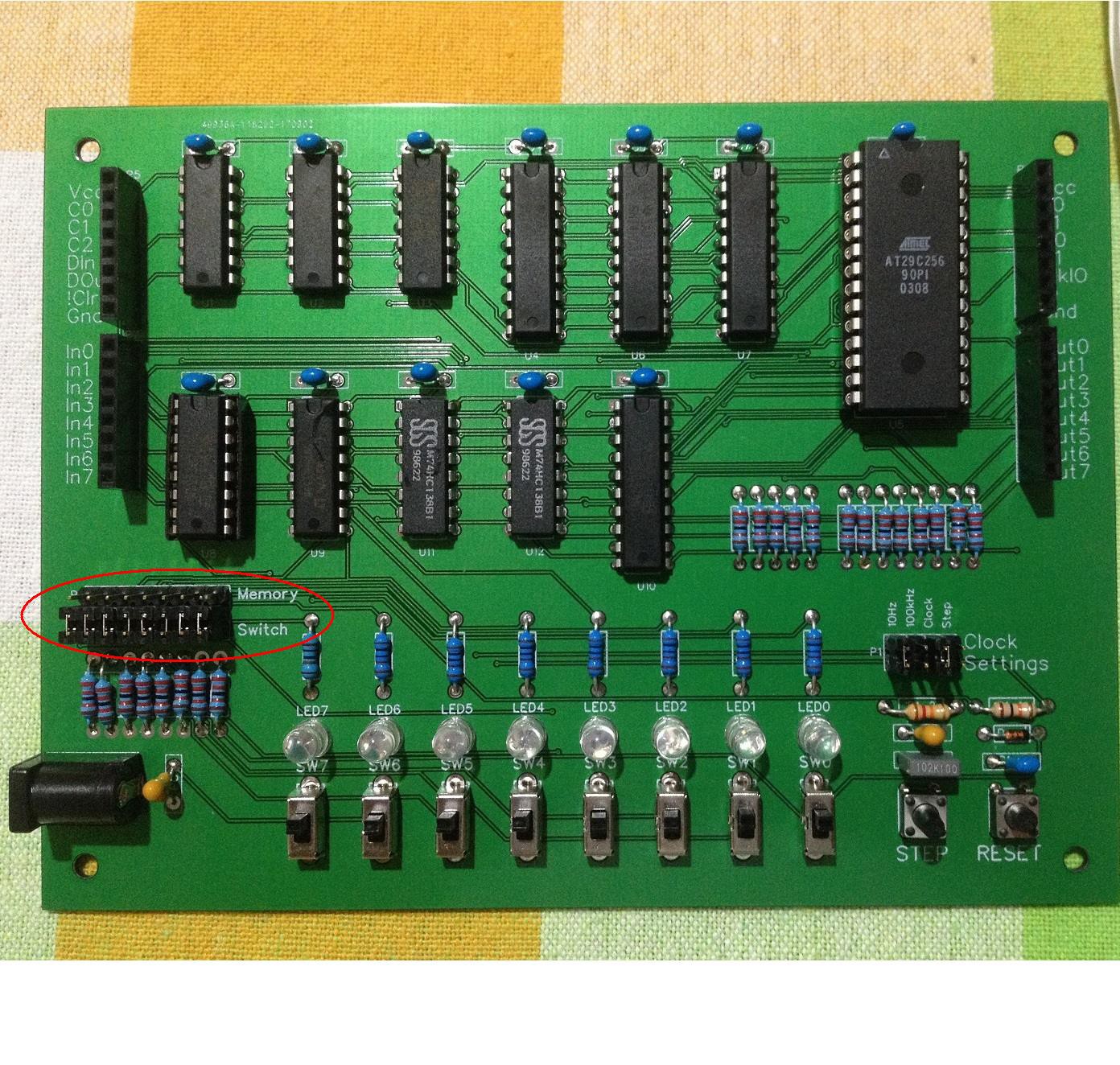
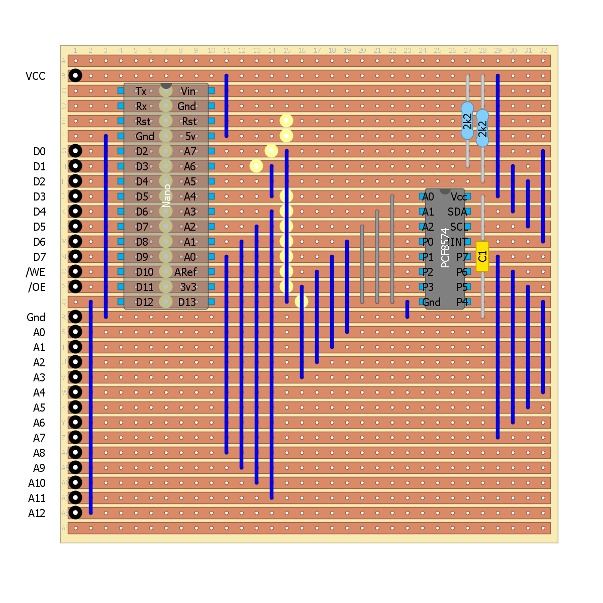
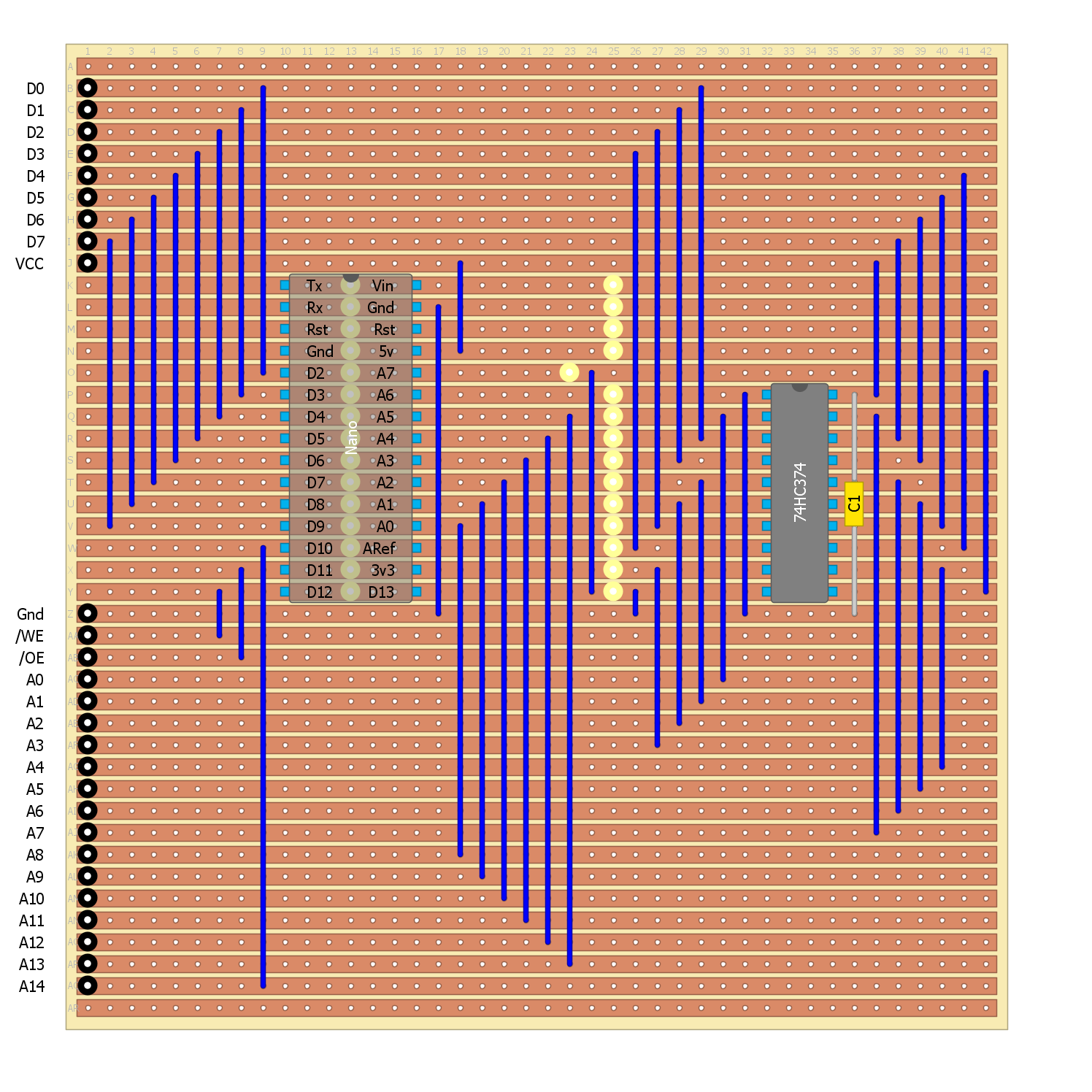
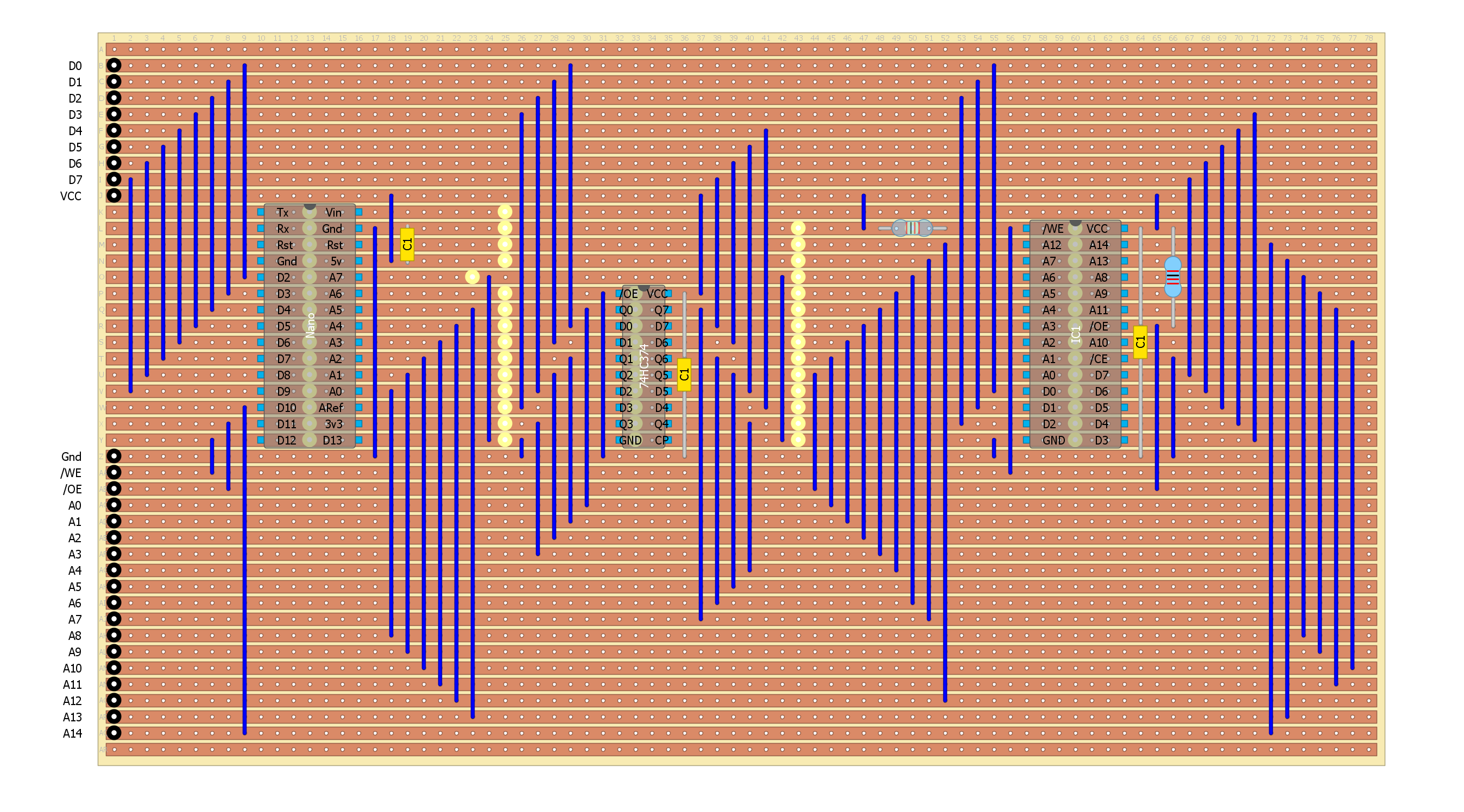
Now your project is an interesting and perhaps useful application for a one bit CPU.
Well done.
Regards Alan