 agp.cooper
One Bit Block Diagram
Here is a block diagram of the one bit CPU I want to design:
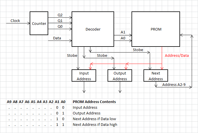
What I am doing different here is using the previously duplicated Input and Output addresses as separate Input and Output address. This gives 256 possible Inputs and 256 possible outputs instead of 16 inputs and 16 outputs. To do this a need a four phase clock and some decoder logic to select the correct Next Address (i.e. depending on if Data is low or Data is high).
Truth Table
Here is the first pass truth table:
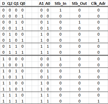
It first pass because small changes can make a bit difference to the decoder circuit.
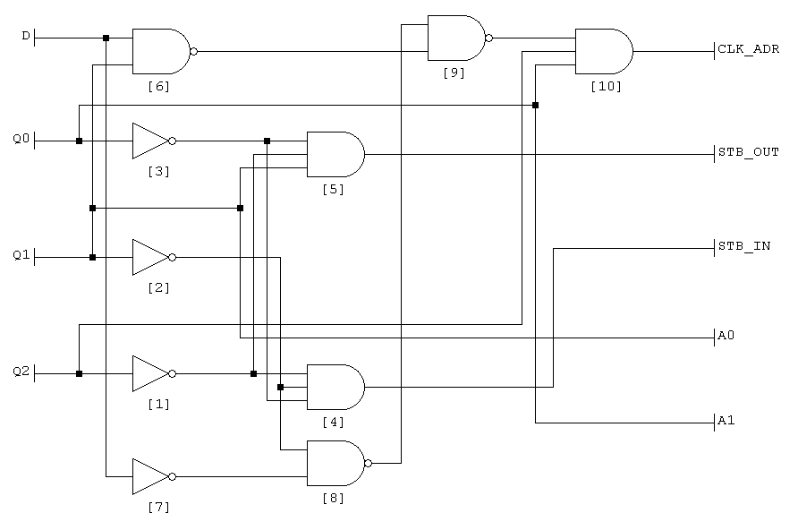
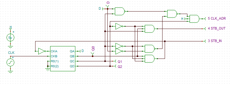
Here is the resulting circuit:
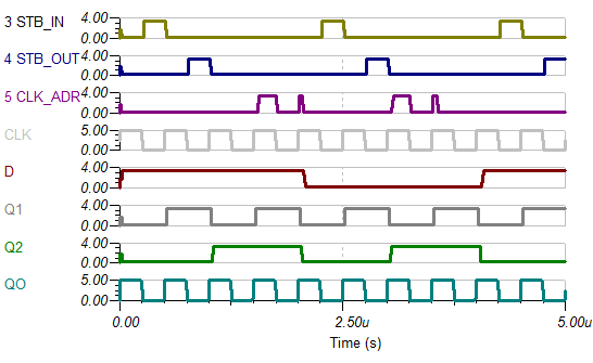
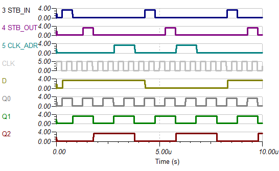
Testing the circuit in TinaTI (looking for glitches) and yes glitches were found on the CLK_ADR signal:
Playing around with the schematic and clocking the Data (D) signal, all good:
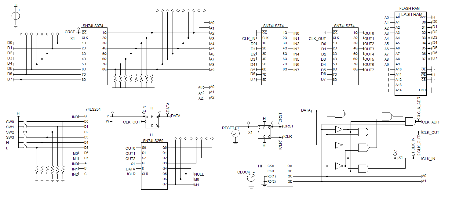
Here is the final schematic:
Ignore the inverter feeding into the CKA of the counter, it is only used to generate a "D" signal.
Conclusion
Is it worth the effort? The old design needed two chips, but not enough gates for the clock and reset logic, and this design needs four chips with enough gates left over for the clock and reset logic. The new design will also need an additional clocked latch for the input/output. So eight chips versus ten for a theoretically better system. The down side is that the improvements are unlikely to be used.
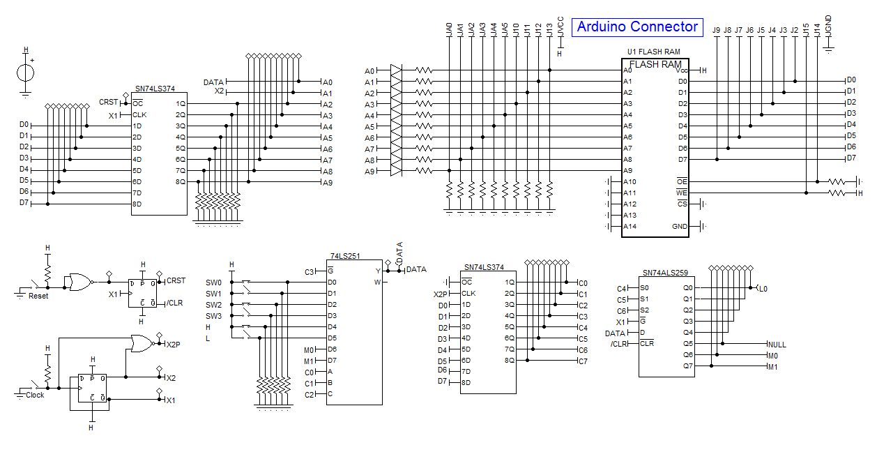
Here is the old design for reference:
Update
Reworked the decoder a little, it seems to be working as expected:
Regards AlanX
Discussions
Become a Hackaday.io Member
Create an account to leave a comment. Already have an account? Log In.