 agp.cooper
The Laughton Electronics One Bit Machine
The Laughton Electronics one bit machine is very likely the smallest discrete CPU that can be built (http://laughtonelectronics.com/Arcana/One-bit%20computer/One-bit%20computer.html):
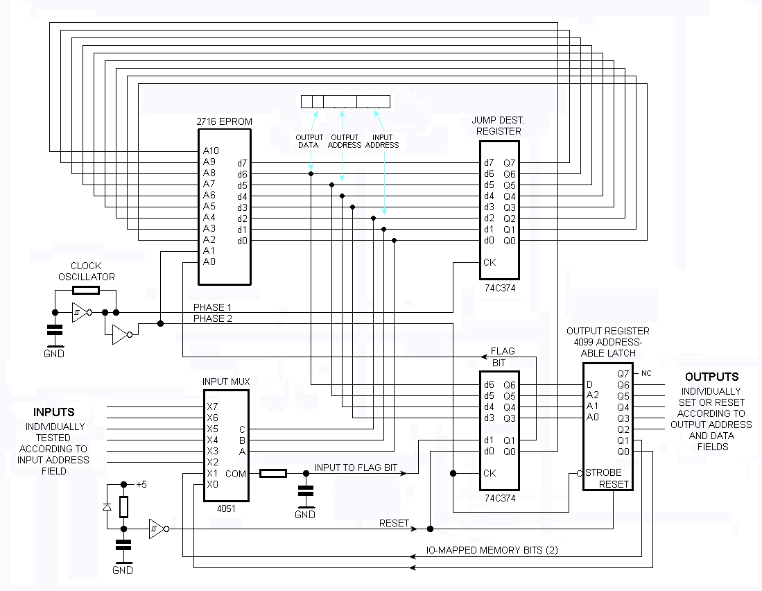
I have designed a simplified version that does not use the data bit in the instruction byte or requires the top half of the ROM to have jump on reset instructions:
(Don't build this, it is not final!)
The reset signal (RST) is clocked or synchronised (CRST) and turns off the address latch. The resistors set the reset address (0x00 in this case). As the clock is still running the instruction at the reset address is executed repeatedly.
My version will probably still need the deglitch (i.e. low pass) on the data line, (I am guessing that the ROM is generating address glitches).
I have taken a Subleq approach here and have a specific I/O address for Low and High. Like Laughton I have added two memory bits.
How does the memory addressing work?
To understand the memory addressing consider typical set of instructions:
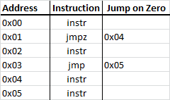
In the above, the next instruction (address) is automatically done in a hardware.
In the Laugthon machine there is no program counter so the next address must be explicit:
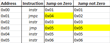
The cost is that the approach costs additional memory.
Here is the Laughton format:
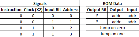
You cannot actually change the input address based on the input bit (as it could oscillate) but you can change the output address. Really, to avoid programming difficulties (in your head!) it would be best to keep for both input bit cases, the input and output address the same. It would also simplify programming if one of the jump addresses is the preferred "next" address (say jump on one).
For my CPU, here is my programming template with some coding examples:
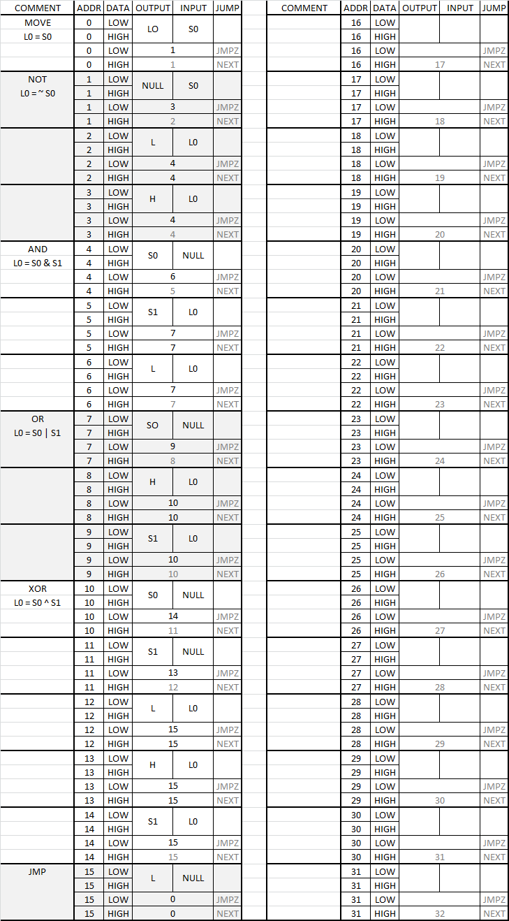
Note: Each row is a byte in ROM (merged cells are duplicated, so each instruction is 4 bytes.
You may see that a more sophisticated CPU would use the duplicated I/O address to extent the CPU I/O addresses and/or add OpCodes.
I am sure that many people look at the Laughton's machine (and download the image) but not knowing how to program it, just move on. The programming template makes it much more straight forward.
OpCode Density
The concept describes the amount of memory required to code something. Simple CPU usually have low OpCode density. Subleq for example is at least twice as bad as TTA (Transport Triggered Architecture), all other things being the same.
Laughton's machine has two functions or instructions and has a higher OpCode density than my version (which is pure TTA). The MC14500B has 16 instructions and the code density would be in the order of four times less ROM space than my machine.
So there is merit in considering an ALU in the bit path (at the cost of I/O addresses). For a single OpCode bit Laughton's approach is hard to beat.
Update
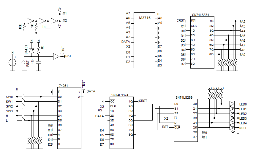
Spent half the day playing around with a strip-board version but decided I needed to get it working in TinaTi. Here is the working TinaTI schematic:
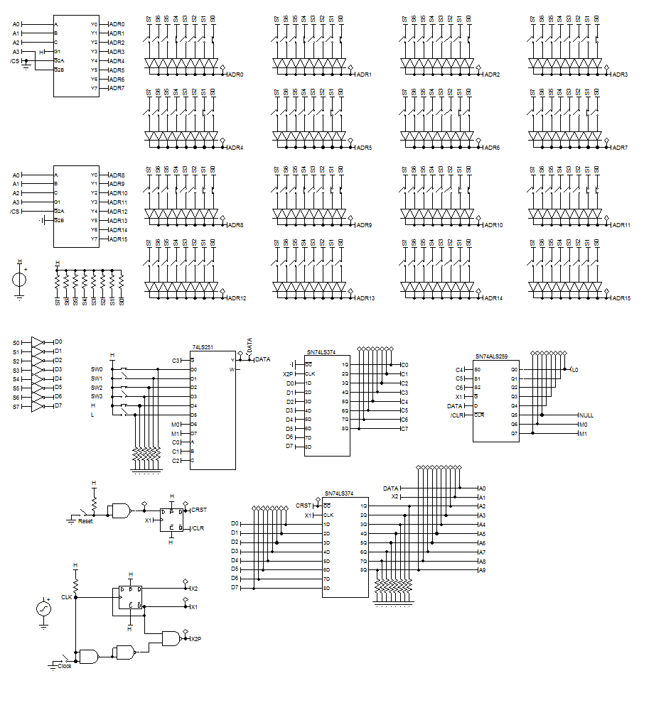
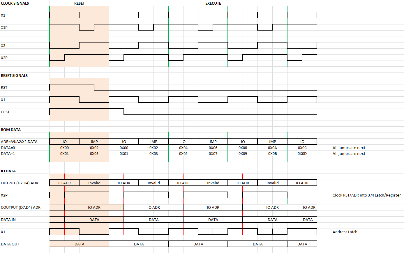
At the top is a hardware ROM! Most the work was getting the clock timing right for the reset. Here is the timing diagram:
Some thoughts on Laugthon's version. As it relies on slow ROM so it may not work with modern very fast PROMs. That is what the RC delay filter is for, to keep the data around so it can be clocked/latched. Anyway, in exchange for two additional chips, I don't have to program the top half of the PROM with reset instructions and the full IO address (8 bits) latched for the cycle. I was playing with a design that separated the two IO bytes but it was starting to get complicated. Overall, seven chips and a clock (i.e. eight chips) still makes a pretty small CPU.
A Second Update
Further work but using a Flash RAM for the ROM. The idea here is to program the Flash RAM in-circuit with an Arduino. This schematic should work but further work is required:
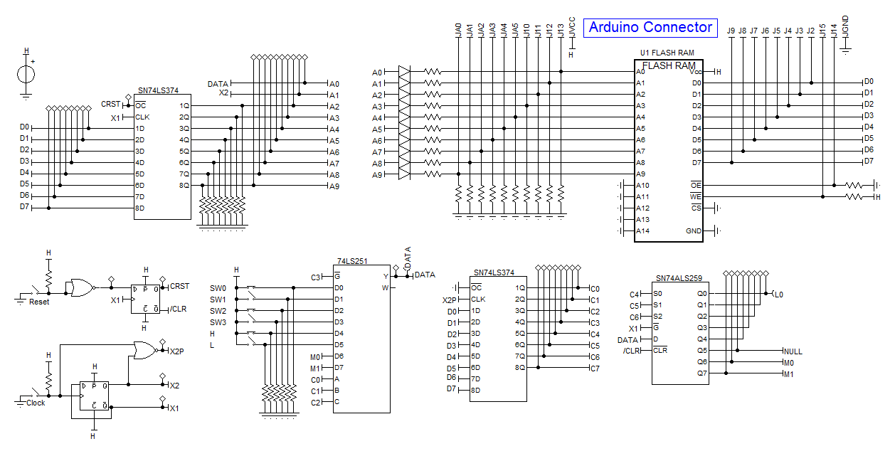
This one bit CPU has 4 inputs, high (H), low (L) and two memory bits (M0 and M1). It has five outputs, null and the two memory bits. It has been tested in TinaTI except the 74LS259 model does not work.
If I build it then the thought shifts to what to use it for as a demonstration? One thought is a bit counter. That is to count the number of inputs pushed and to write the binary result.
AlanX
Discussions
Become a Hackaday.io Member
Create an account to leave a comment. Already have an account? Log In.