 agp.cooper
Version D
Still paying with the design, usually this means that the design is not done.
It's just something you know and can not explain, i.e. "You can do better!".
So yes, Version D is much better:
Improvements:
- Used the spare I/O byte as page memory (cost two chips), I can now access all the memory on the PEROM (that what the datasheet calls the Flash memory).
- Used bit 7 of the IO byte to set the output high or low rather than read a high or low input.
- Used bit 6 of the IO byte to determine if the I/O is read or write (cost two decoder chips).
- So I can read and write up to 64 inputs and outputs (base board has six inputs and outputs and two memory bits).
- The design is very simple!
- For the PCB design I can add a port for expansion of additional I/O as required.
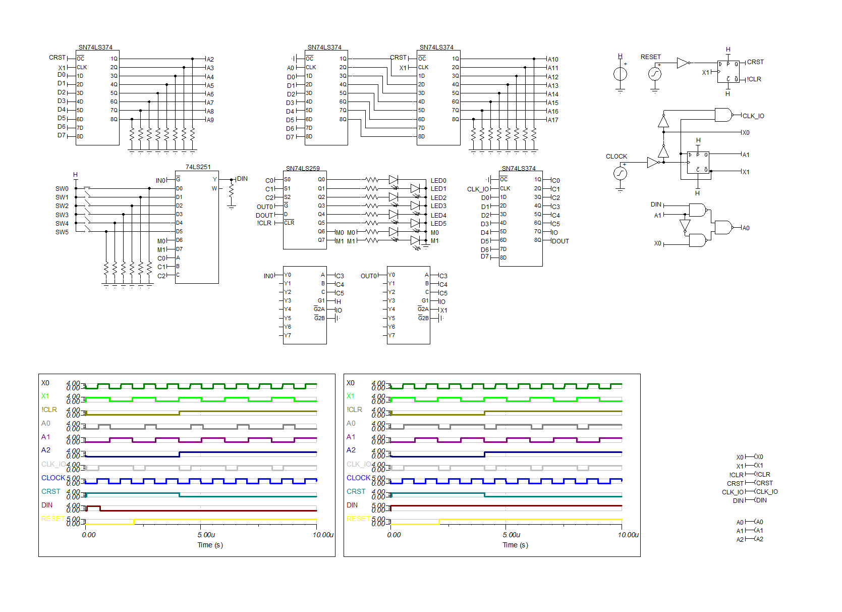
The timing diagrams basically show the relationship between the signals, the address decode based on DIN high or DIN low and that the signals are glitch free.
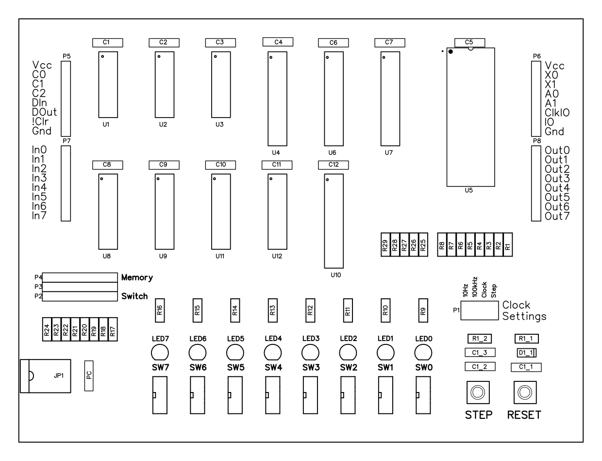
PCB
For the PCB I have used jumpers to switch between memory bits and input switches, and provided expansion ports (... well you never know!). The PCB was a bit of a rush last night so the layout could be improved but it is been fabricated now:
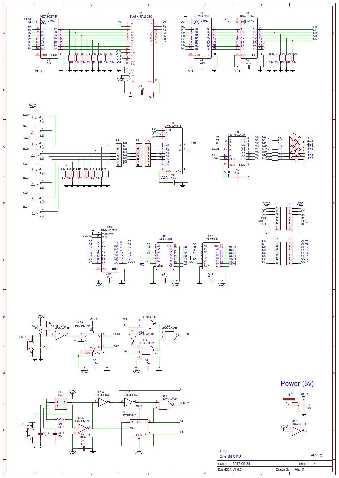
Here is the schematic:
Including postage the PCBs (for five) cost US$33, you cannot complain other than I only really want one PCB.
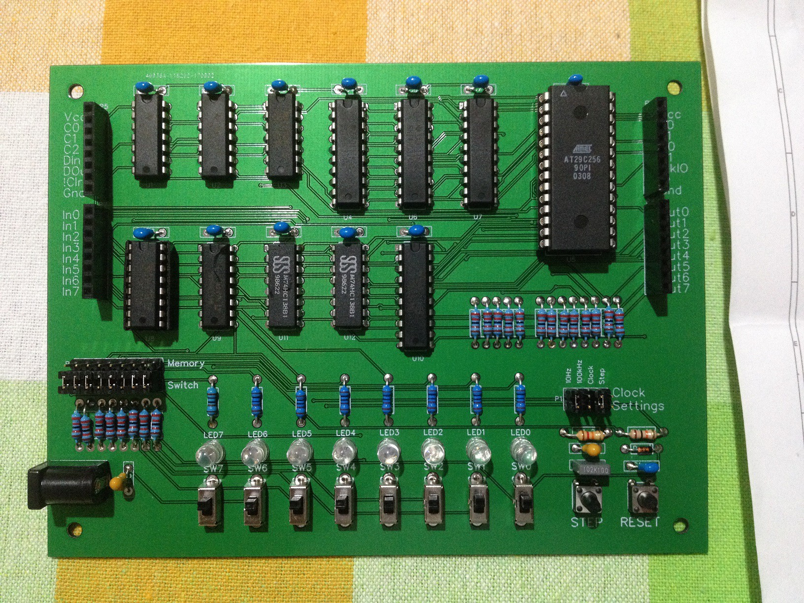
Assembled and Waiting a Programmed Flash ROM
Here is the assembled board. I must have been in a rush as the components are all over the place!
AlanX
Discussions
Become a Hackaday.io Member
Create an account to leave a comment. Already have an account? Log In.