 Luke Valenty
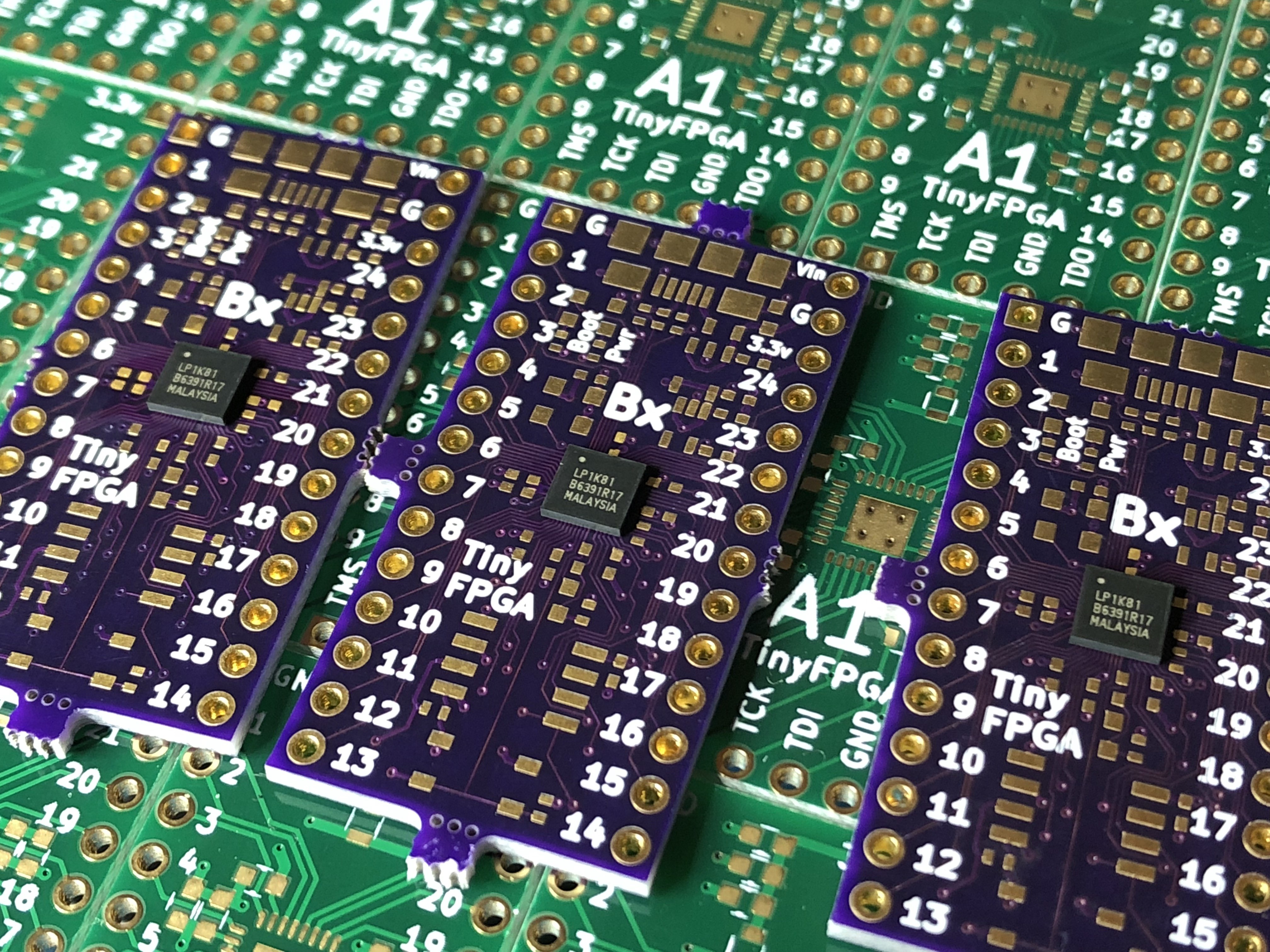
I had a very exciting few days as I received some TinyFPGA BX prototype boards from oshpark. I didn't really think I'd be able to assemble these first prototypes. I had expected that it would be too difficult to reliably reflow the FPGA onto the new footprint. I also wasn't sure that the boards would be high-enough quality since I was pushing the design to the very limits of what oshpark can do.
So I scrounged up my USB microscope and took a look at the PCBs just for fun.
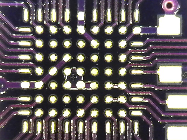
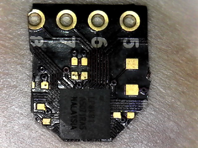
Ohh my glob. They are perfect. Each one of the 6 prototypes I received from oshpark are absolutely immaculate. This was the first time I ordered 4-layer boards from oshpark and I am impressed. The soldermask pull-back is just 0.05mm. That's just 50 microns. The circular pads are 200 microns in diameter and the pill-shaped pads are about 330 by 100 microns. I realized these boards were good enough to try out.
I had a bad experience using solder-paste and a stencil when I assembled the original B2 prototypes. It was very difficult to get a clean print and then it was difficult to get a reliable reflow. This time I decided to use nothing but flux and a hot-air gun. The flux goes on footprint spread thin, then the BGA package, then the hot air. It took about 30 seconds to reflow. The first board I reflowed using this method was sacrificed for science.
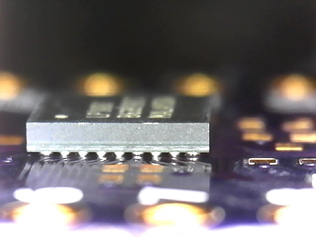
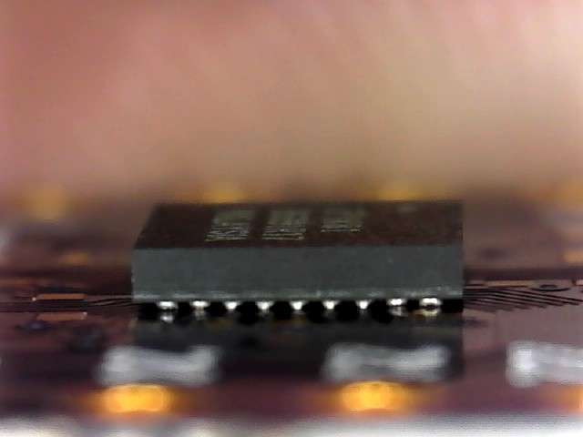
I wasn't sure how well the balls would reflow onto the footprint so I hacked away at the assembled board to get a good shot of the balls.
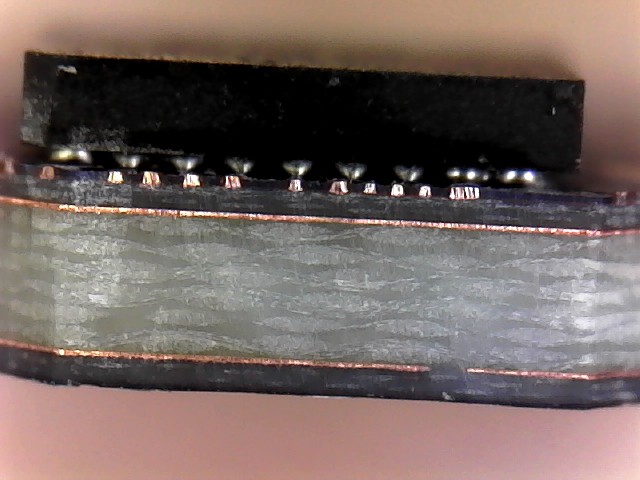
Looking at the balls we can see one solder ball on the left edge and two on the right edge that are on circular pads. The rest of the balls are on pill-shaped pads pointed towards the camera. You can clearly see the difference in shape. The balls seem to be reflowing onto the pill-shaped pads very well.
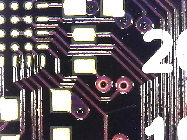
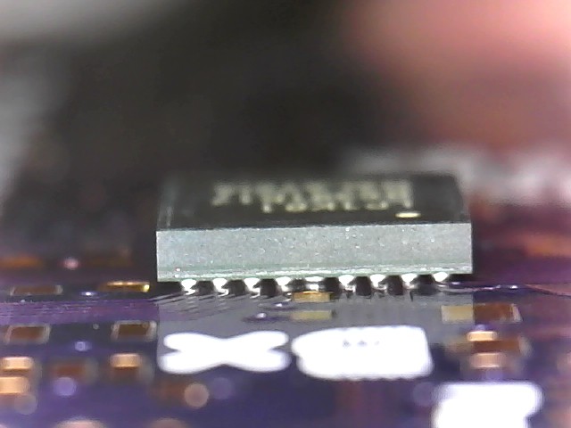
I tried sanding and cutting into the BGA package itself to try and get a cross-section of some balls. This didn't work out too well as debris was pushed underneath the package and the solder balls may have been pushed around.
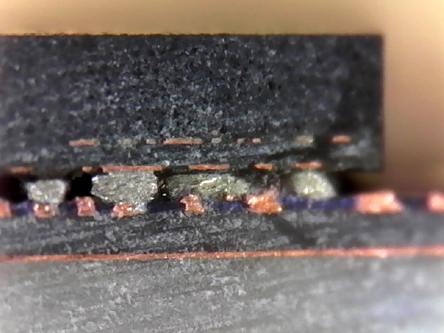
Talking about this on Twitter, there were a few suggestions from the community on better ways to analyze BGA package reflow issues. Without an x-ray, the best option seems to be dying the area under the package and letting it set before pulling the package off vertically. If there is dye covering any pad then you know you have an open.
My next step was to assemble some boards by hand.
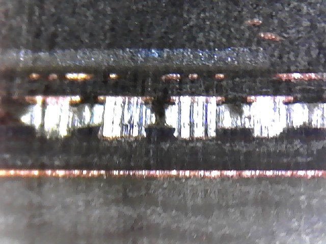
I started out by reflowing the FPGAs onto three boards. Without cutting into the board I was still able to spy some very promising connections on all four sides.
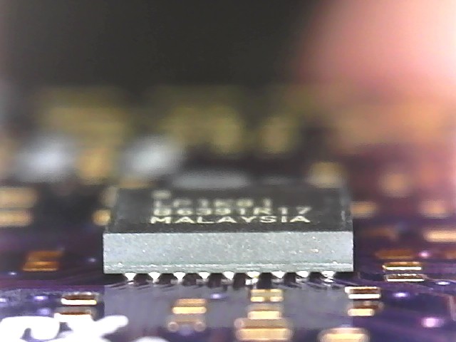
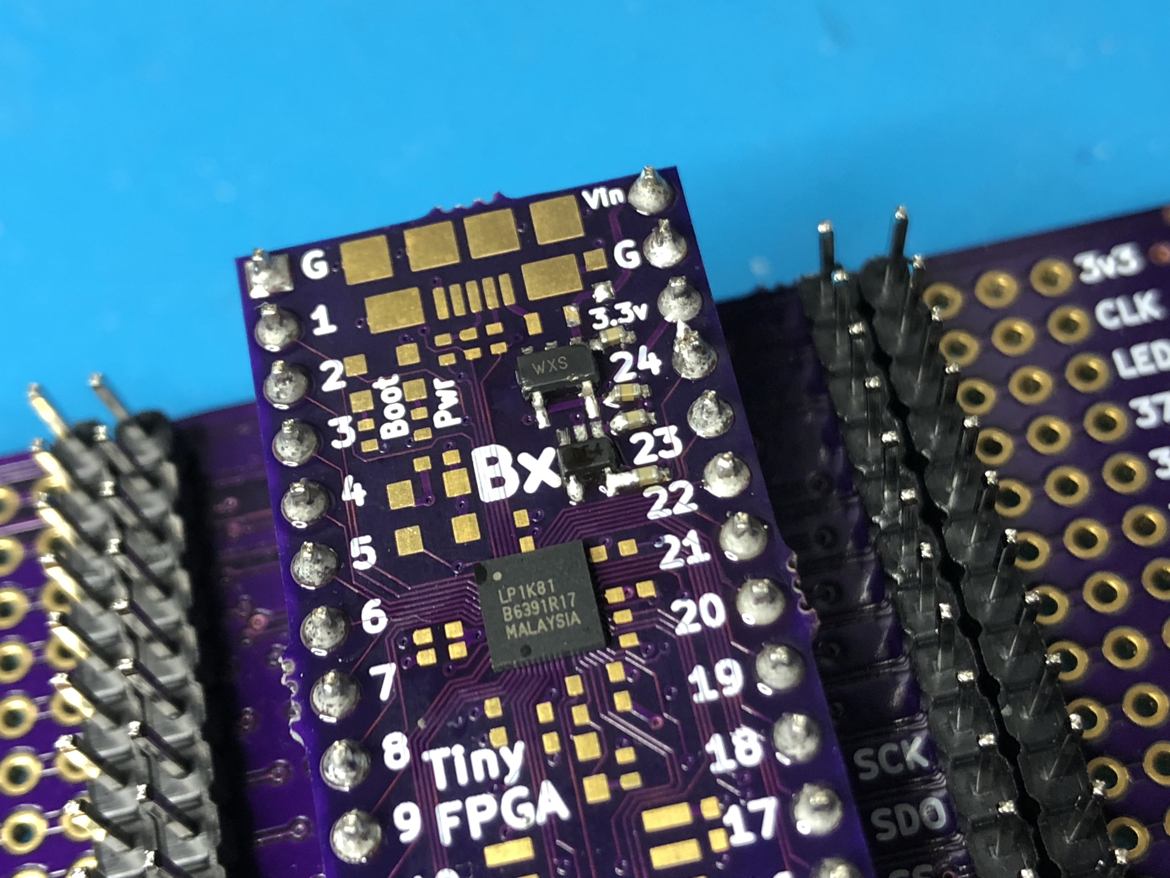
This was getting very exciting. I believed this footprint would be very risky, but each board was turning out better than expected. I was interested in testing the basic functionality of the FPGA and the connections to all of IO pins. Testing this basic level of functionality meant that I could pick and chose the critical set of support components necessary to breathe life into the chip. This ends up being the two voltage regulators, their capacitors, some bulk capacitance, resistor for PLL VCC, and the SPI flash. Since I would be assembling these few boards by hand this would save me a lot of time.
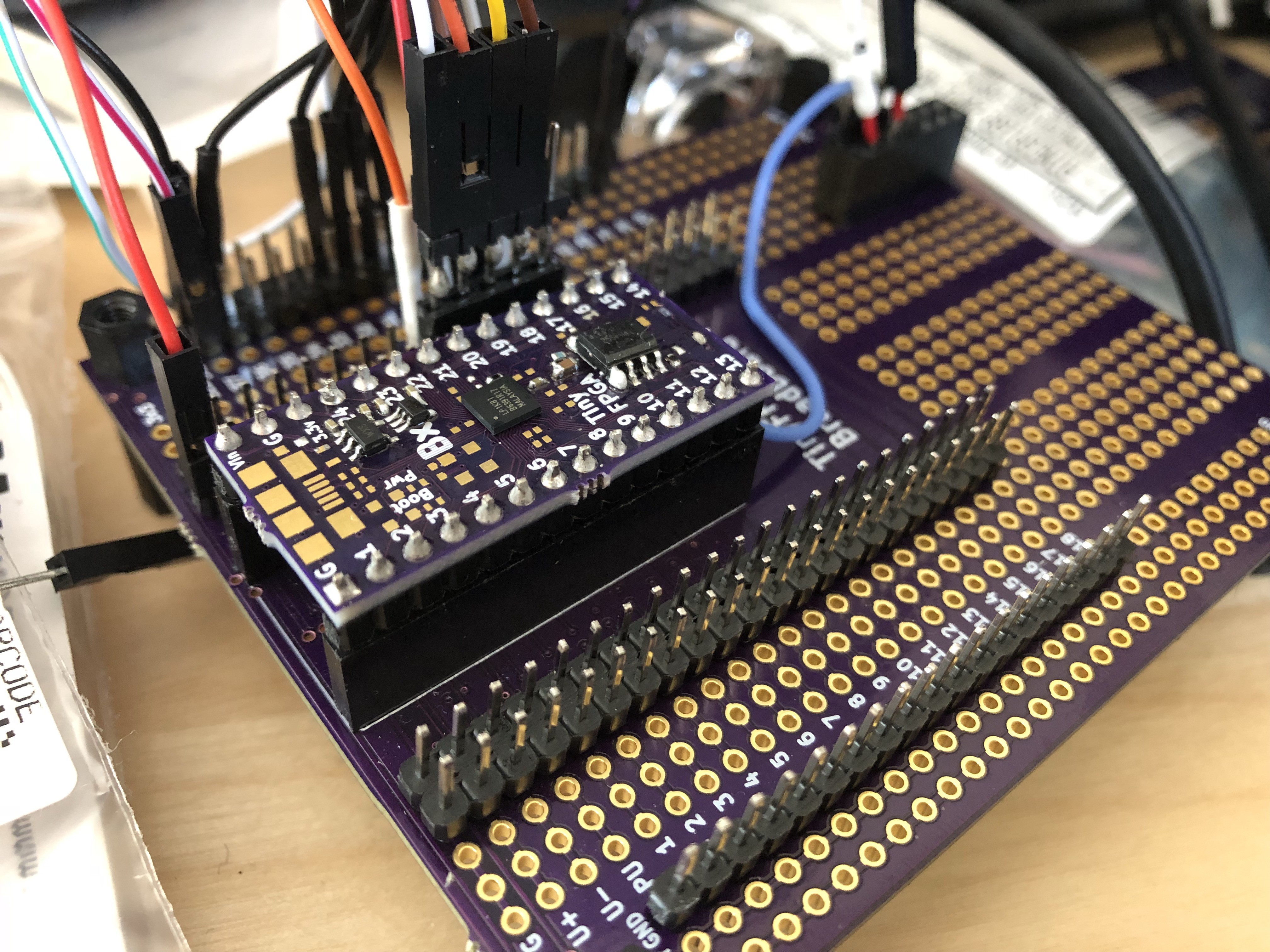
I also decided that the first order board I had to bring-up would require a lot of debugging. So I soldered on a full set of BX pins so I could put it into a special breadboard designed for the BX boards.
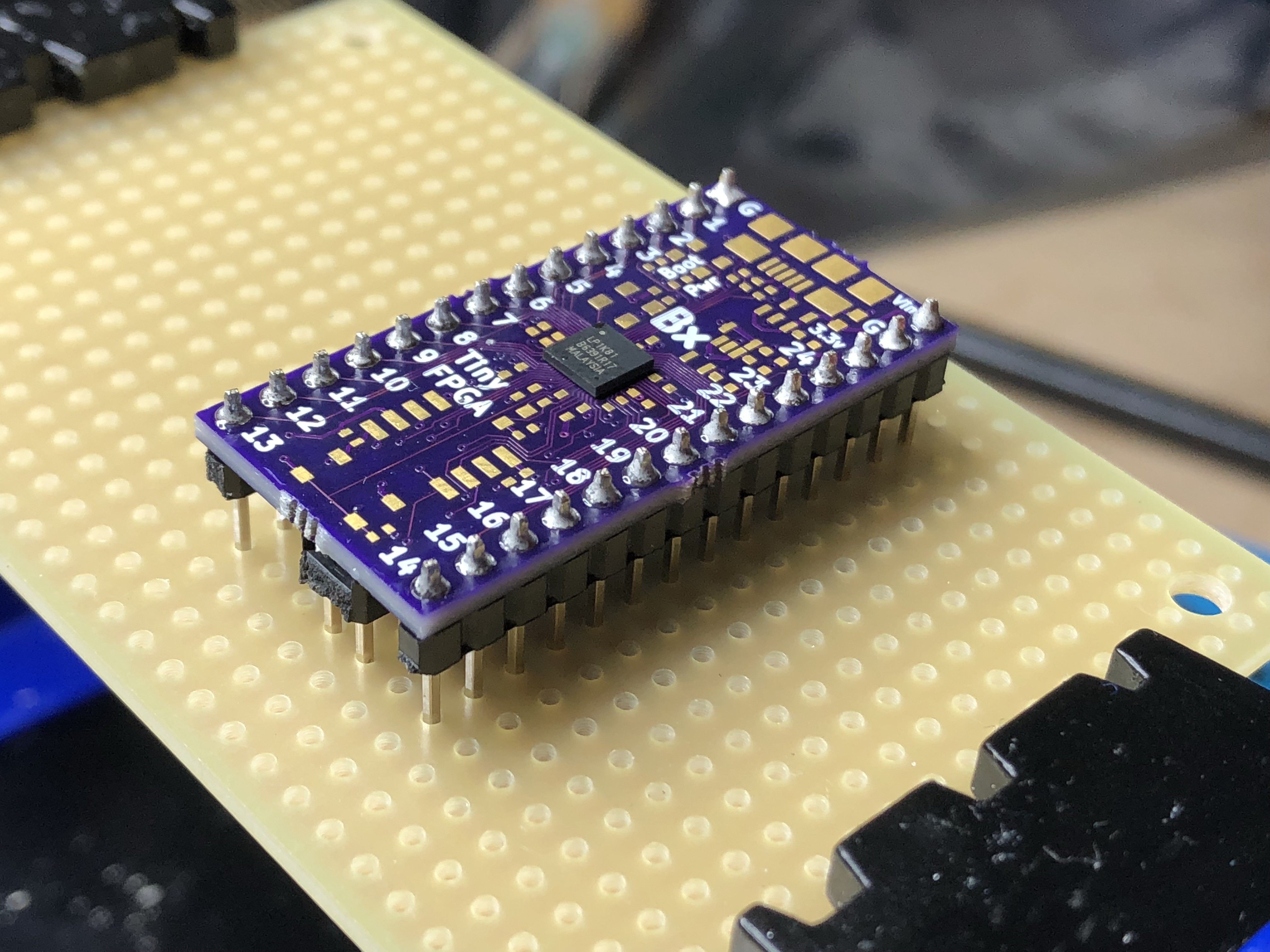
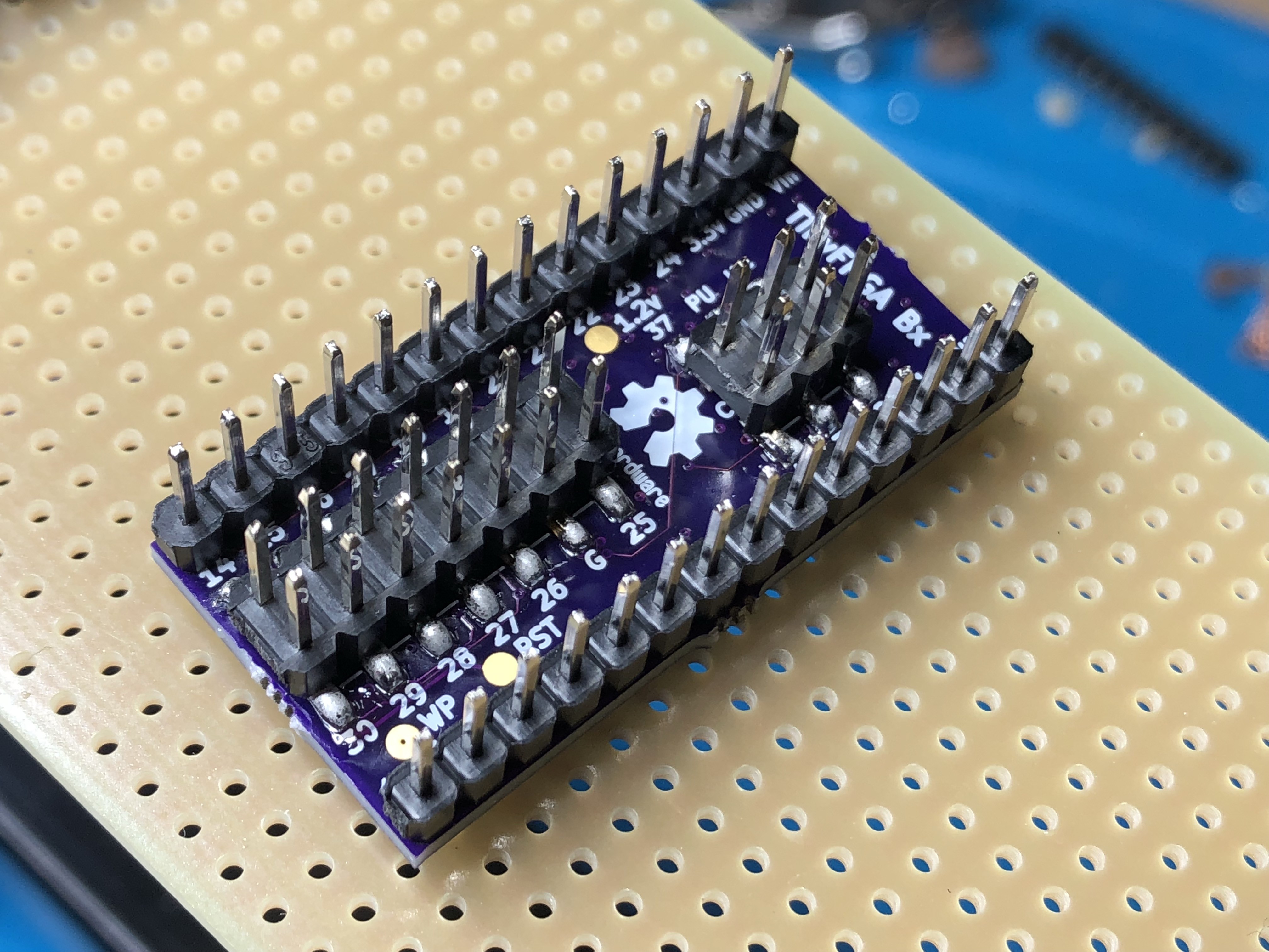
The breadboard has all of the IOs routed out to their own rows. I soldered on some headers that my logic analyzer and lattice programming cables could attach to. This provided a nice platform for first bring-up.

Here's a close-up of the voltage regulators:
The mini "testbench" with the programmer and logic analyzer connected. The blue wire is soldered onto a test-point used to hold the FPGA in reset. This is needed to program the SPI flash.
After a few false starts I finally got the FPGA programmed and booting from flash:
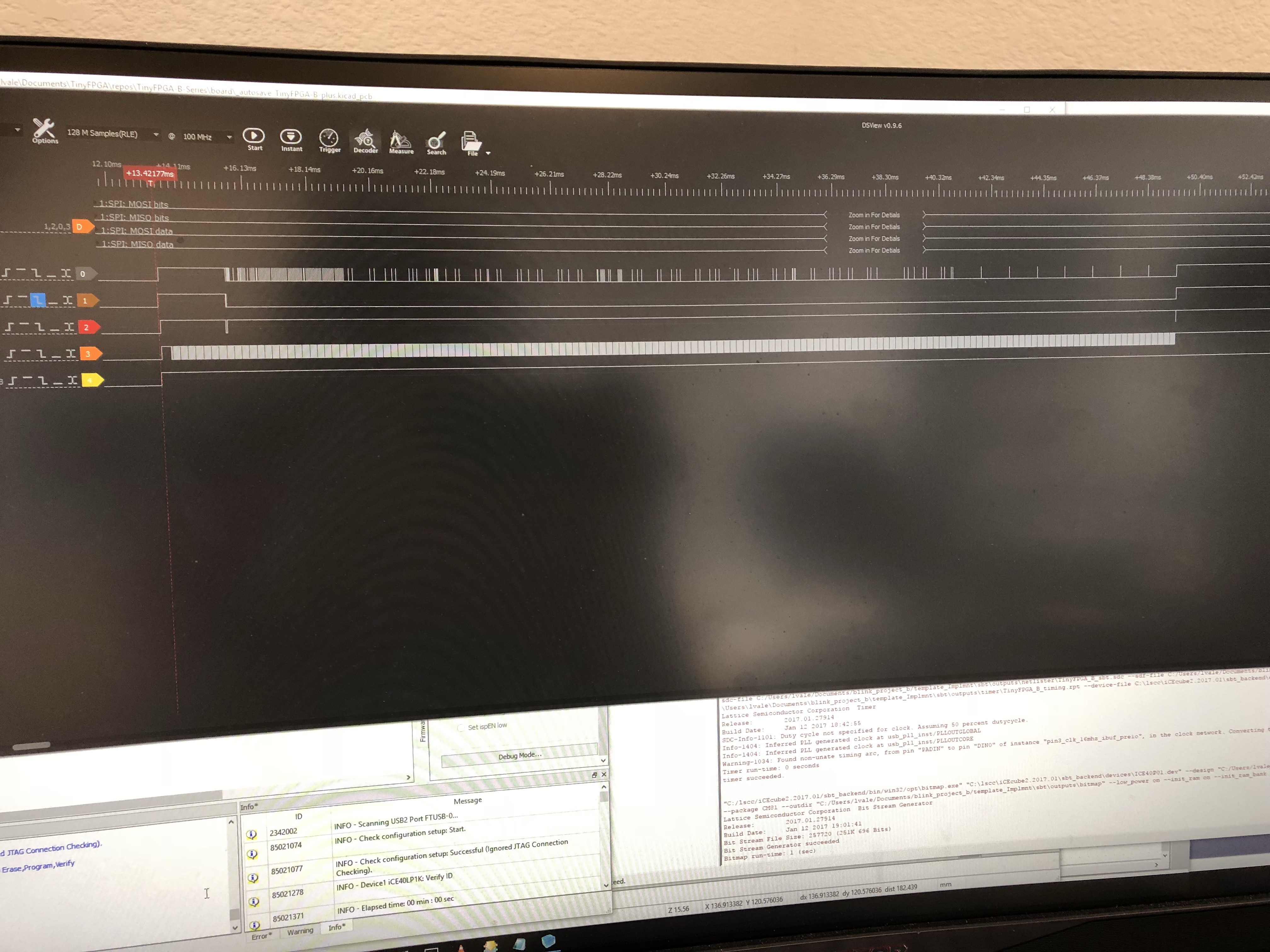
The waveform is captured from the SPI interface between the FPGA and flash memory. The flow is simple: the FPGA wakes up the flash, reads starting from address 0x00000000 until the end of the bitstream, then puts the flash into a deep sleep mode. Success!
Well, that's what it felt like at the time, but there was still more work to do. The breadboard helped me get the FPGA up and running, but now I need to checkout all the pins. I had also received my test-jig boards from oshpark, but had so far only assembled a pogo-pin version.
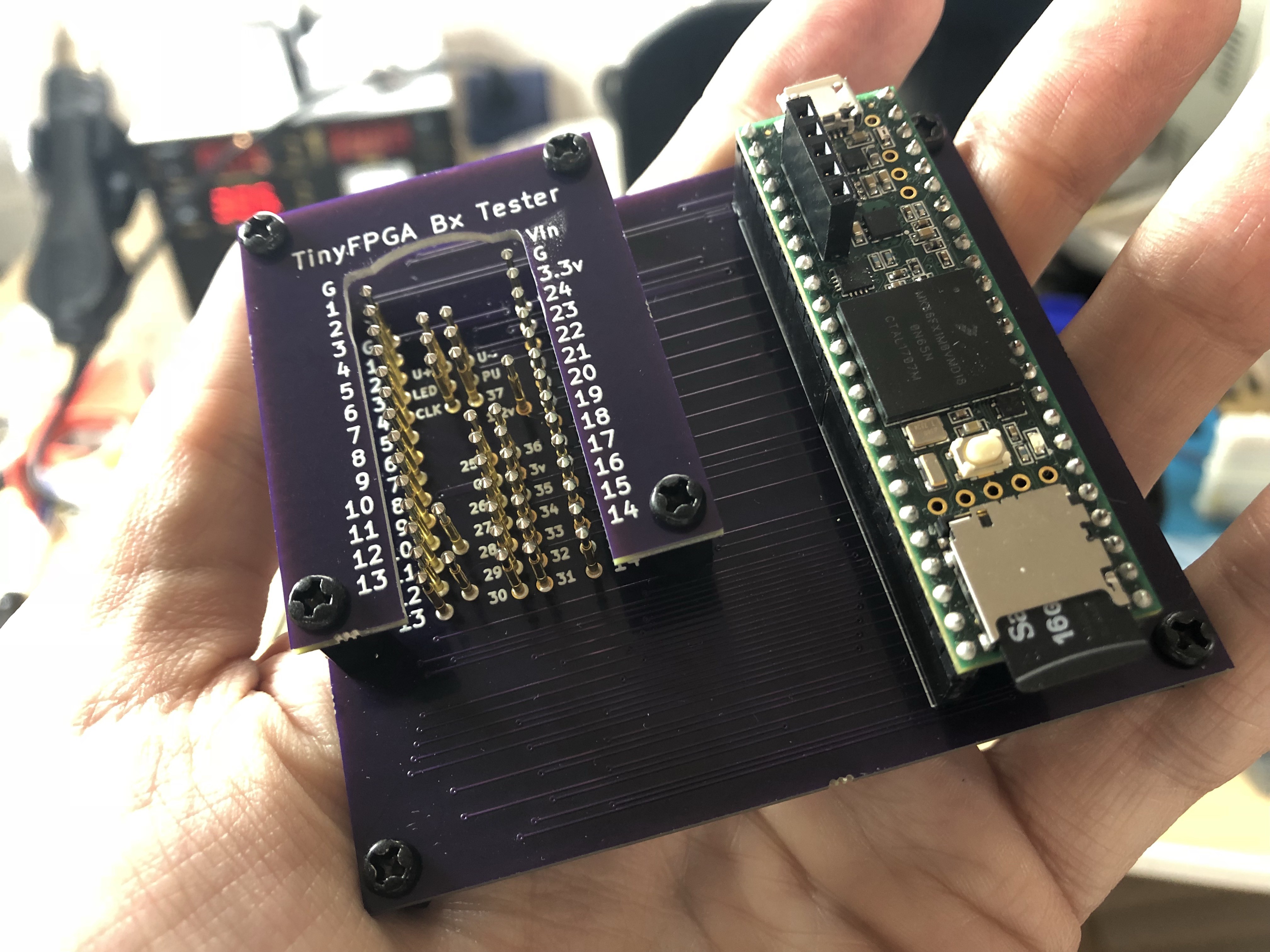
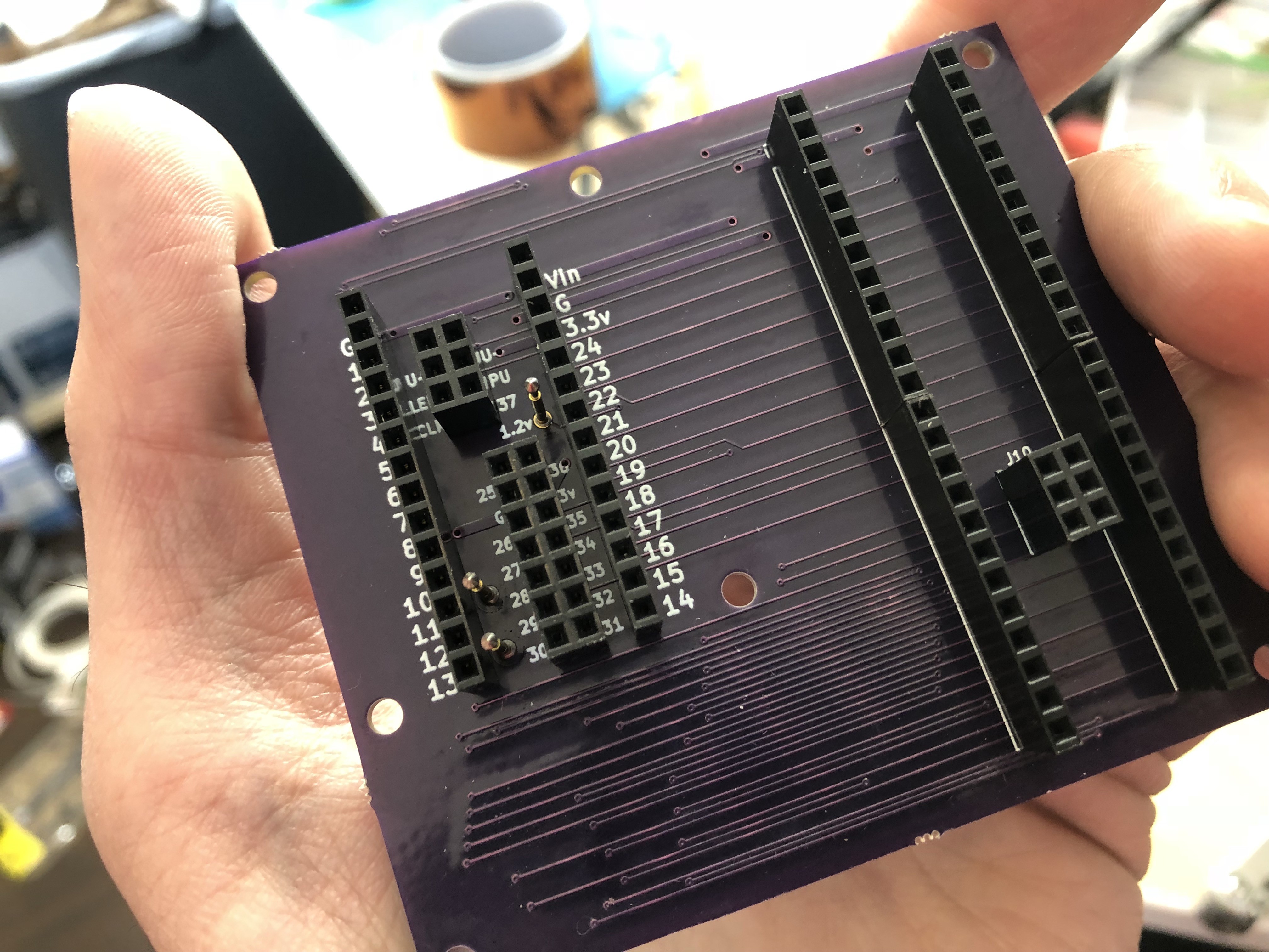
While super-useful for testing boards coming back from the assembly house, it wasn't going to work for a board with pins already soldered. I didn't quite feel like assembling another BX board yet, so instead I assembled a version of the tester that has sockets for the pins. This would be useful in the future when I need to test boards with pins before shipping them out.
For the three test-points on the bottom, I soldered on some pogo-pins as usual. This ended up being very useful. Not only can I check-out the reliability of the first prototypes, I can also port the testing firmware from B2 to BX and get all the bugs worked out. Cool.

I was able to port the firmware over and discovered a problem. There were some shorts in the tester board itself. Not a bad problem. It would have been worse if the shorts were on the BX module itself. But this means that the socket-based tester couldn't test 100% of the pins. I had done most of the work to get the tester and test firmware up and running. Now was the time to assemble the other two boards.

They didn't work well at first. If you look closely near pins 23 and 24 you'll notice the capacitors for the LDOs are missing. I thought I would see what would happen if they don't have their capacitors. Nothing good happens. The 1.2v rail was too high and the 3.3v rail was too low. They were way out of spec and the tester failed them on the power supply every time. Good news: the tester works. Not so good news: I still had to solder on the capacitors.
Now I have two boards without pins that can go in the pogo-pin tester.
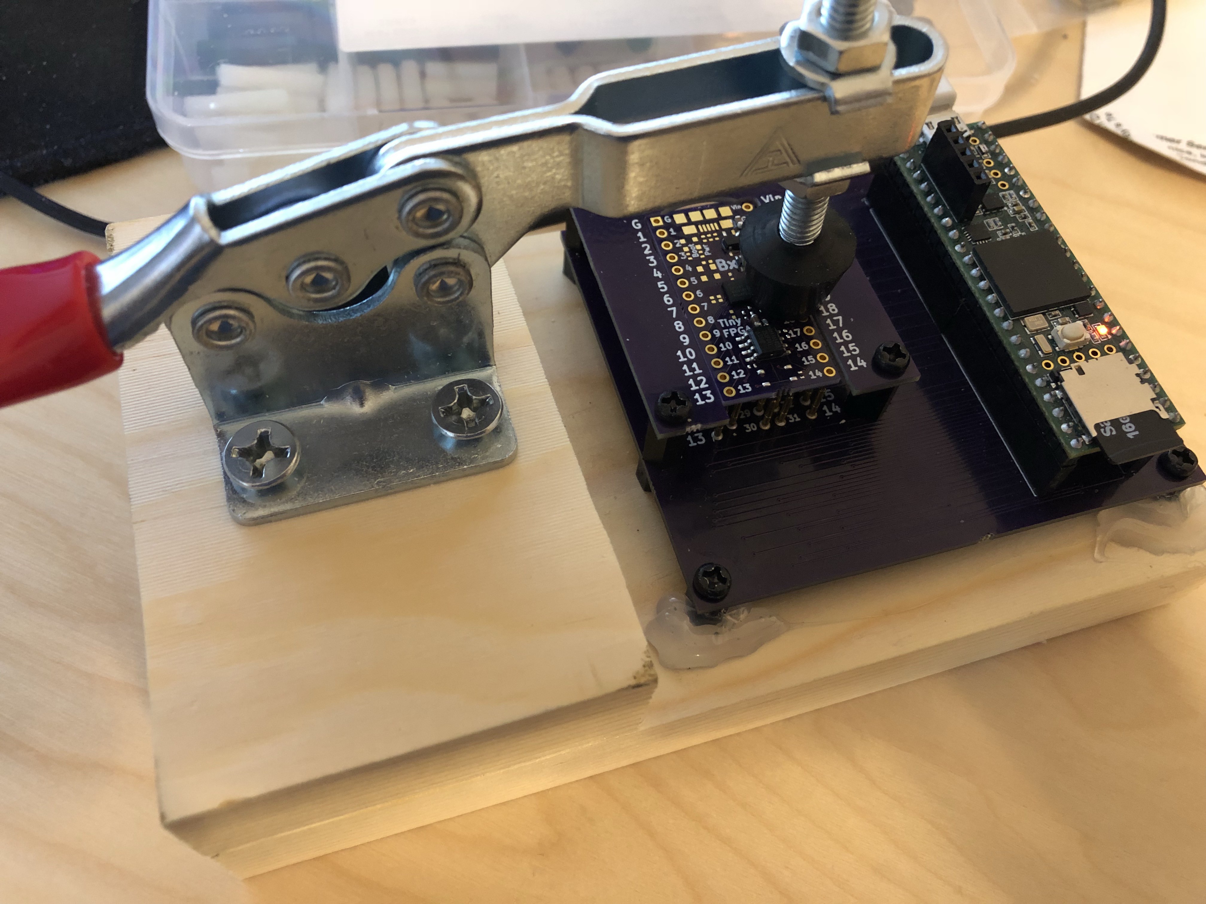
The old B2 tester required me to hold down each board for about 18 seconds. This ended up being very painful for all 250 boards of the original manufacturing run. I had pledged to myself then that I would find a better solution. That solution is a toggle clamp. Once its in position it stays down. Much better.
There are no buttons or indicators on the tester itself. It connects to a computer and displays results on a text terminal. To keep the test process easy and fluid for the operator, it is completely automated. The only action the operator needs to do is to clamp and unclamp boards. The tester automatically detects a board by sensing the 3.3 volts from the voltage regulator.
Once a board is detected, the tester waits a moment then goes through a comprehensive test covering all of the active components of the board. The results are output to the terminal as they are generated.
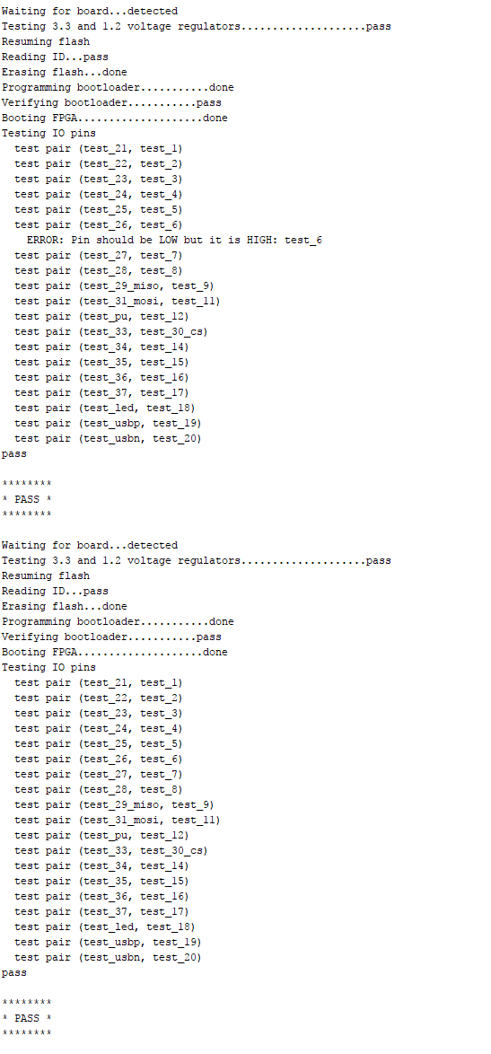
Hmm. The first board has an error. Ohh well, the second looked fine. Well, it was almost like that. Except when I came back an hour later and was playing around with the tester and boards I found that now both boards were failing. This was not likely a board issue, it was a tester issue.
I looked for shorts in the tester, there were none. Of course not...shorts in the tester would cause failures for all boards. It was more subtle than that. The boards were no longer being pushed down evening by the clamp. The clamp rubber "pusher" had shifted out of position over time. I realigned it and retested the boards.
Now it was a success. Both boards passed perfectly. It took a few long evenings but in the end the future of the BX boards is looking very bright. When the 20 prototype boards come back from my manufacturer I'll be ready to test all of them and get a taste for the yield of a production run. With these results its looking very promising.
Keep your eyes peeled for more news and details on a crowd-funding campaign in the next few weeks.
Discussions
Become a Hackaday.io Member
Create an account to leave a comment. Already have an account? Log In.
Congratulations ! good job :-)
Are you sure? yes | no
great write-up!
Are you sure? yes | no
Great result!
Are you sure? yes | no