 Just4Fun
CPLD configuration design (Quartus II)
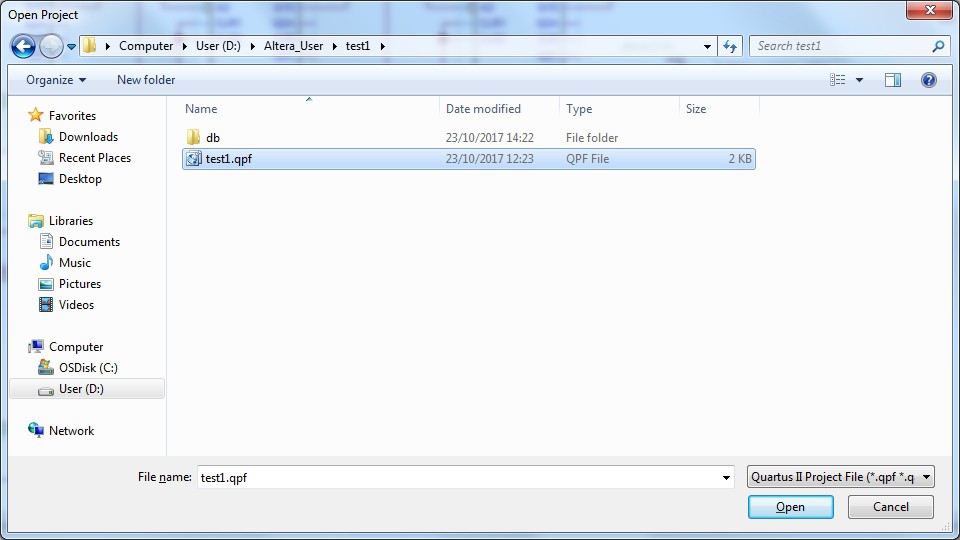
Open yours previously saved project (see previous "Log") from Quartus II with "File" -> "Open Project..." and select the file "test1.qfp". The .qfp extension is used for the Quartus II projects:
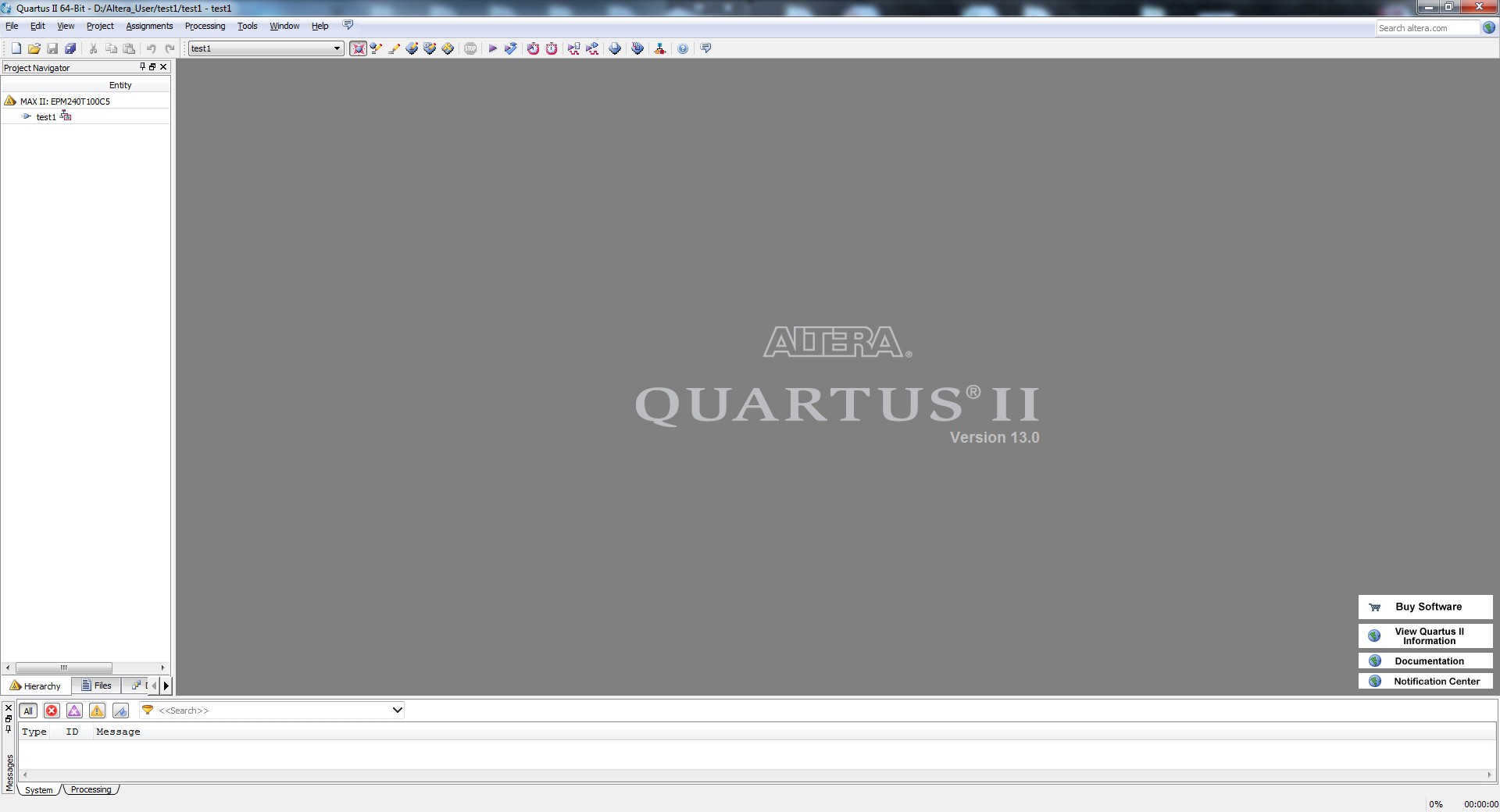
 This is the environment:
Now it is necessary to add a schematic sheet into the project.
From the Quartus II menu click on "File" -> "New...":
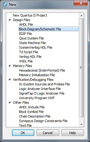
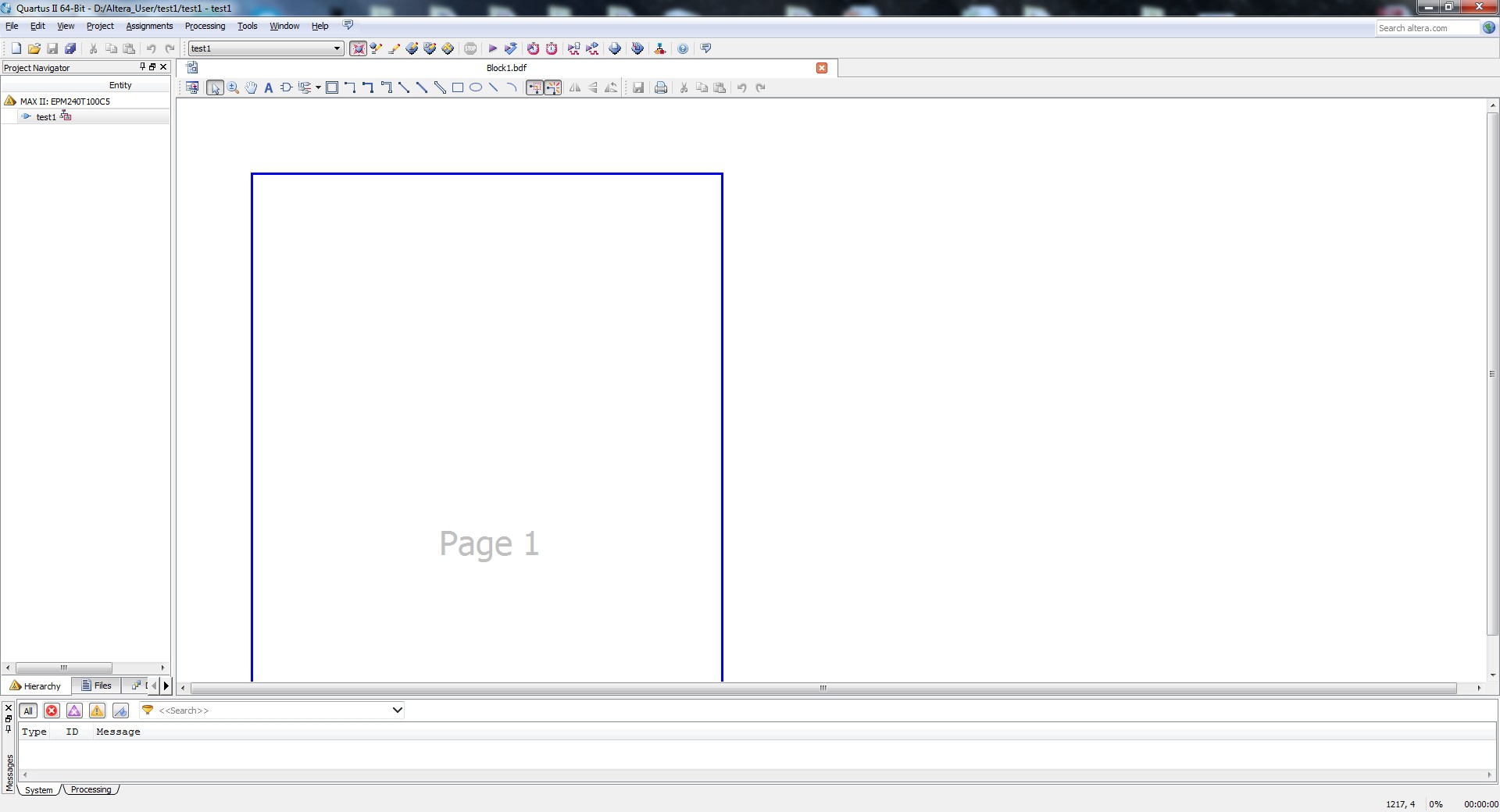
and select "Block Diagram/Schematic File". A new schematic file will be created:
Now it's time to design the needed circuitry to blink a led inside the CPLD.
In this basic example, to make things easier, I'll use the schematic editor and the embedded library that emulate the well known 7400 device family to divide an input 36MHz clock till to about 2Hz. The 36MHz clock comes from the STM32 MCU using the STM32 MCO/PA8 pin (pin 29), that is connected to the CPLD GCLK1 (pin 14) pin . It will be possible see this signal using an oscilloscope connected to the pin 5 of J6 (TEST1 connector) and to the pin 8 of J7 for the GND (TEST2 connector).
Of course to create the 36MHz output clock from the MCU, a sketch must be uploaded into the STM32 flash using the Arduino IDE. In the following we will examine this sketch too.
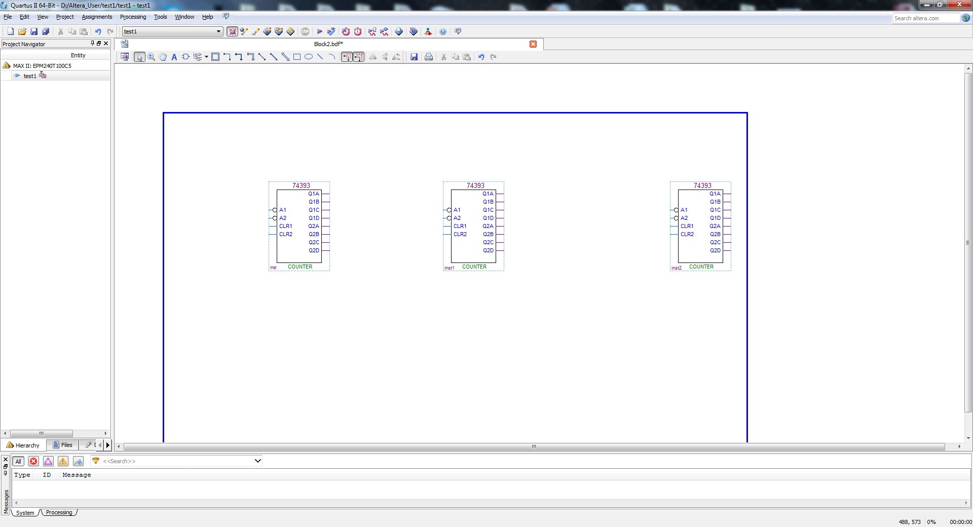
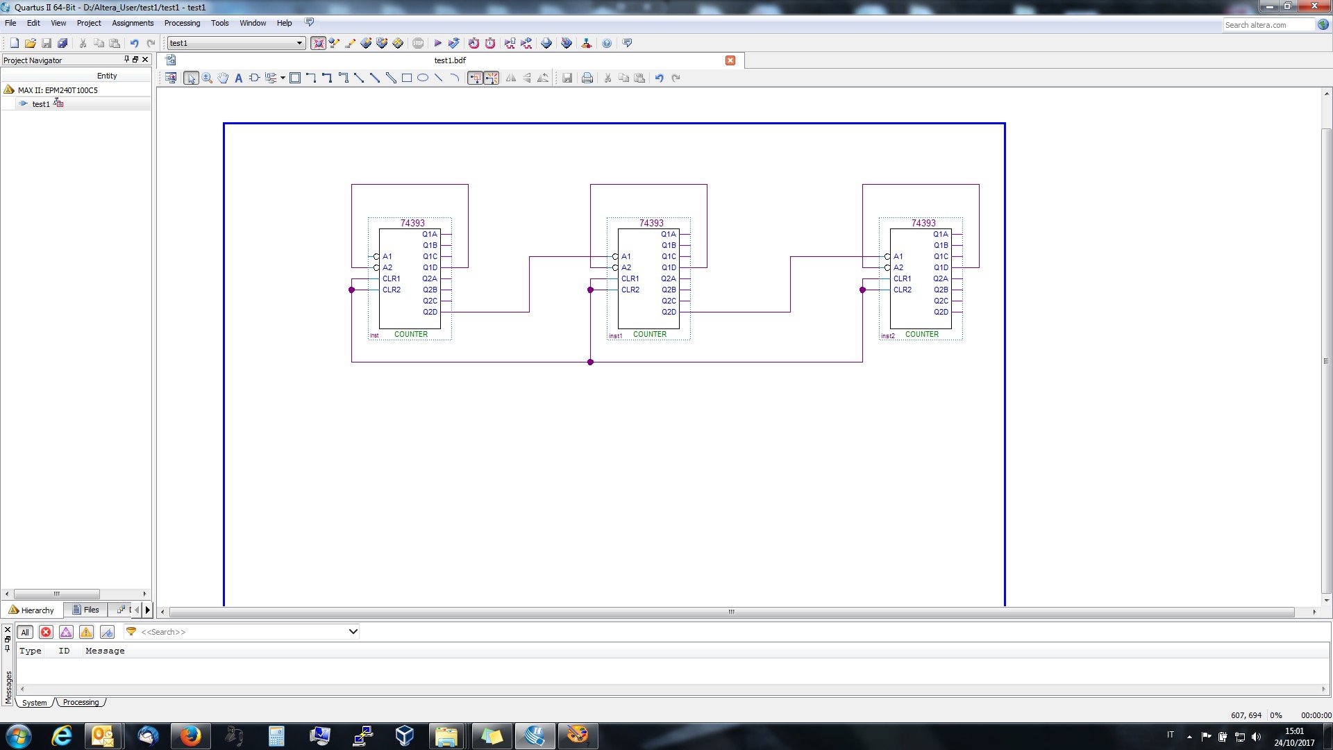
Now I'll use three 74393 counters, each one connected to work as a 1:256 divider.
Form the designer tool bar select the "Symbol Tool":
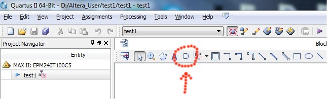
and then type 74393 in the "Name" field:
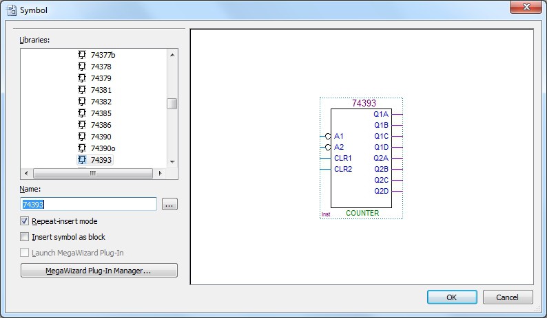
press the "OK" button and place three 74393 in the sheet (use the left mouse button to place):
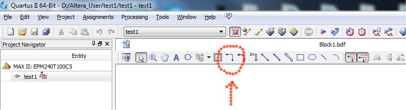
now press the "ESC" key and select the "Orthogonal Node Tool" to make connections:
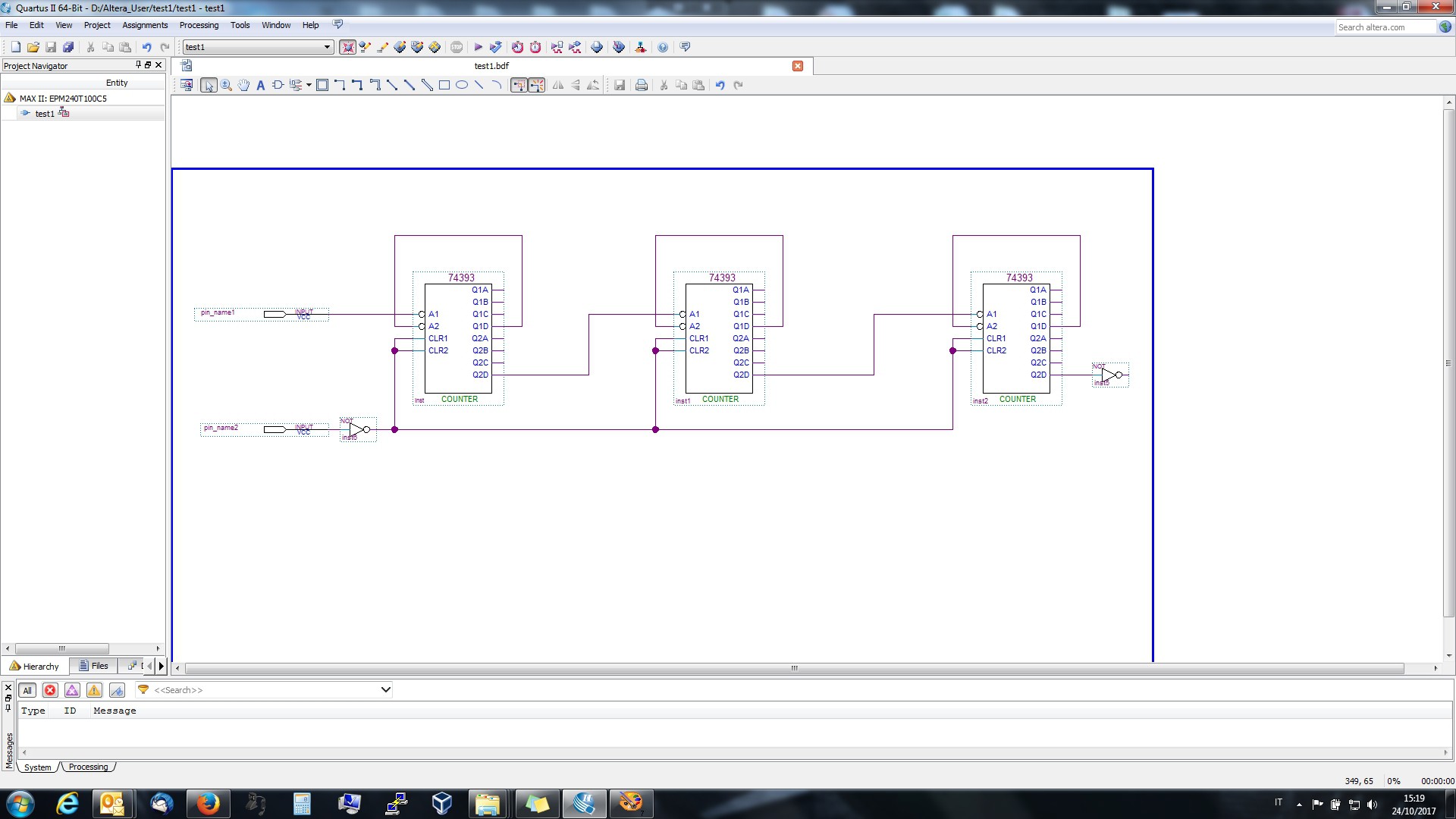
 and complete the connections as in the following photo:
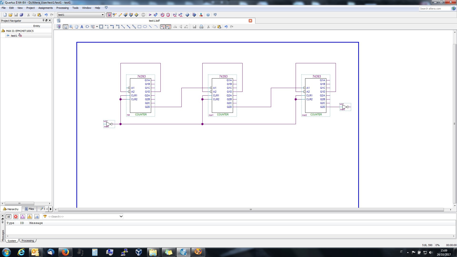
Now press the "ESC" key and select select the "Symbol Tool", then type "not" in the "Name" field:
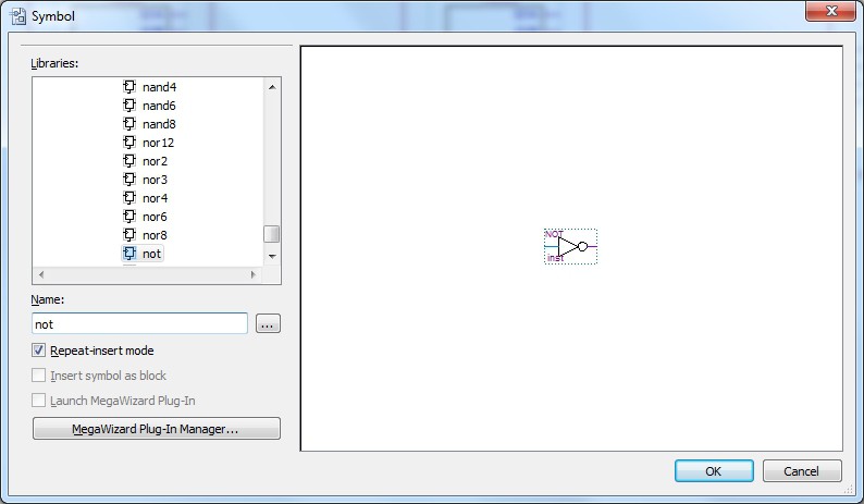
press the "OK" button and place two not in the sheet (use the left mouse button to place) and connect them as in the following:
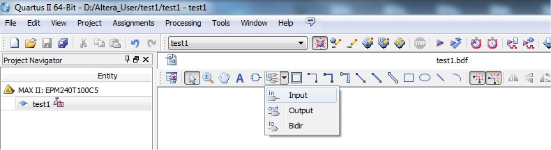
Now it's time to add the input (the input clock from the MCU) and the output (the led to blink). More, I'll add an input key to the Clear function common to the three counters.
So press the the "ESC" key and select select the "Pin Tool" and the "Input" sub-selection:
and place two input ports (as done before) and connect them as in the following photo:
Now I'll add an output port for the led.
Press the the "ESC" key and select select the "Pin Tool" and the "Output" sub-selection:
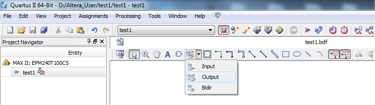
and place an output port (as done before) and connect it as in the following photo:
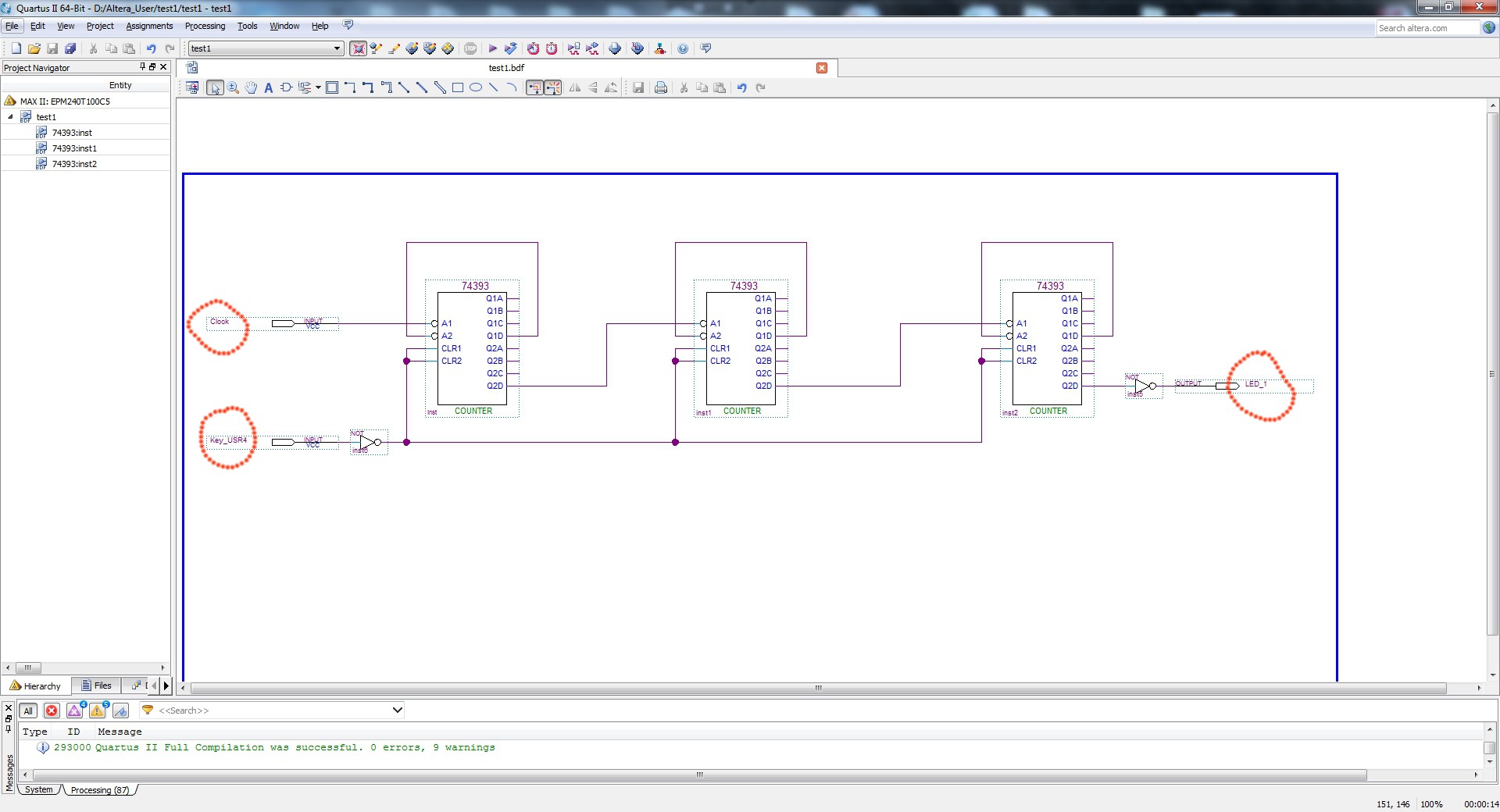
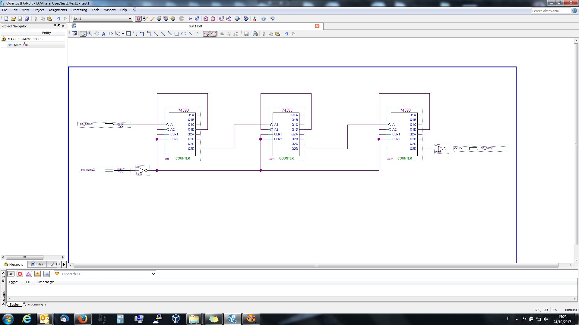 Now rename the names of the input/output pins (pin_name1, ...3) as in the following photo, clicking twice on each name:
Now the schematic entry is done, so save it.
The next step is the association of the input/output with real pins, and the definition of their electrical properties.
Before that it is convenient to do the compilation of the project, so press the "Compilation" icon:
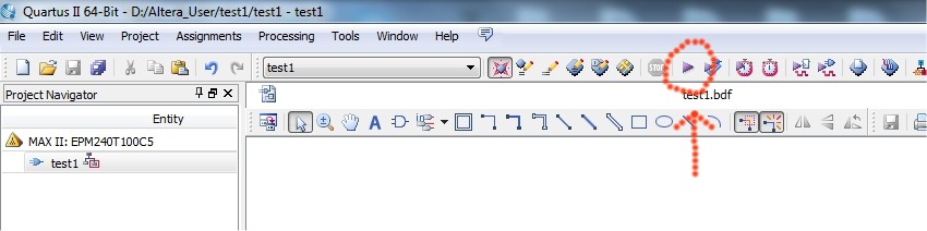
and wait the completion:
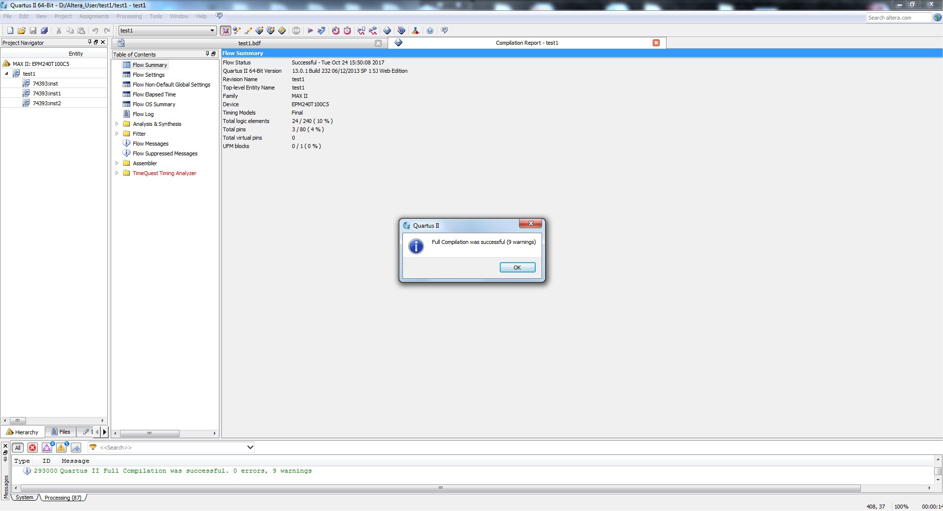
Now press the "OK" button and then the "Pin Planner" icon:
and the "Pin Planner" panel will be activated:
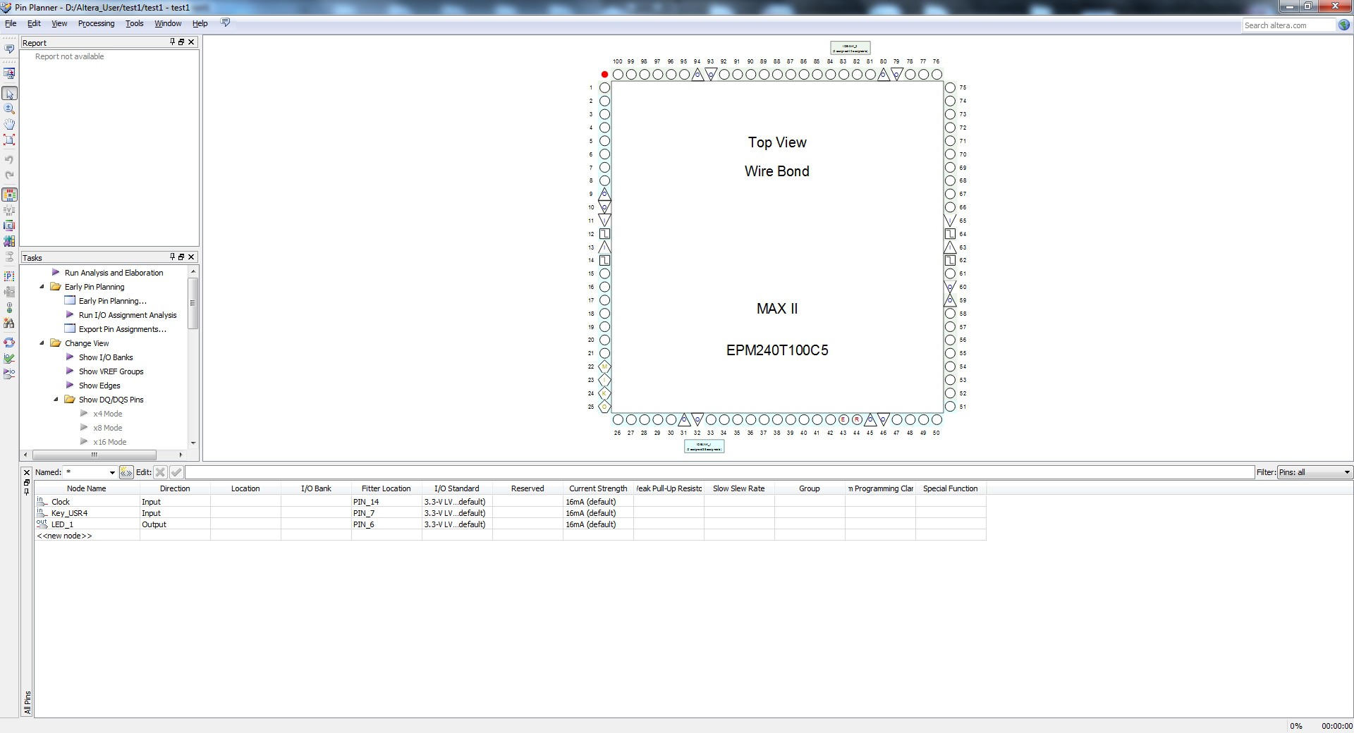
This is the place where to define the CPD used pins and their electrical behavior (e.g. in this panel you can set the internal pull-ups, the maximum current, the digital levels, etc.).
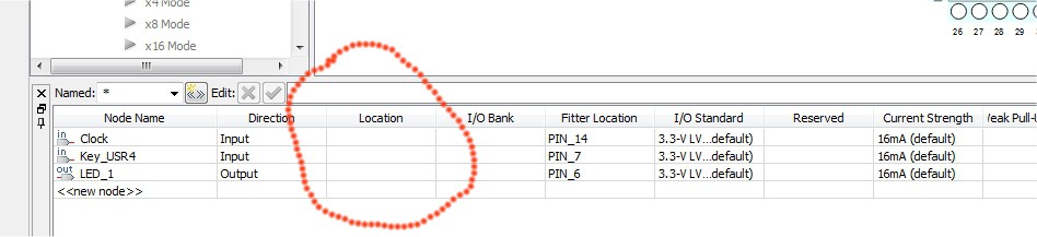
Now set the correct physical pins in the "Location" fields in the bottom panel:
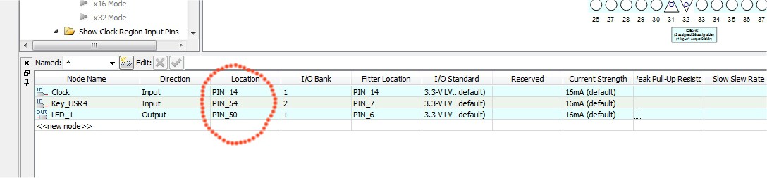
To set the physical pins click on the "Location" field and select the pin to assign. Repeat this for every input/output pin (in this example there are three pins to assign). From the schematic it is possible check that the clock pin (from the STM32 MCO pin 29) is connected to the CPLD pin 14, the USR4 key is connected to the CPLD pin 54, and the LED_1 is connected to the CPLD pin 50. So edit the "Location" field accordingly.
After the editing, the configuration must be as in the following photo:
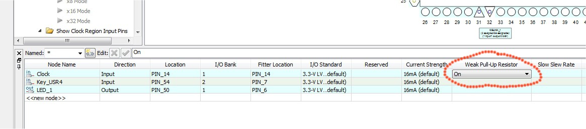
Because the clock is made from the STM32, and in some conditions that pin can be in HiZ, it is better activate the pull-up resistor on pin 14 to avoid any floating state.
To do that click on the "Weak Pull-Up Resistor" and set it to "On":
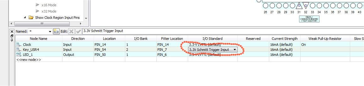
More, you must set the input behavior of the input pin 54 (connected to the key USR4) as a Schmitt trigger because there is a de-bouncing analog circuit on every key.
To do that change the "I/O standard" for that pin to "3.3V Schmitt Trigger Input" (note: if you don't see a column, right click on any column name and select the wanted column to the current view):
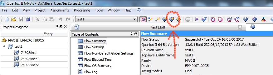
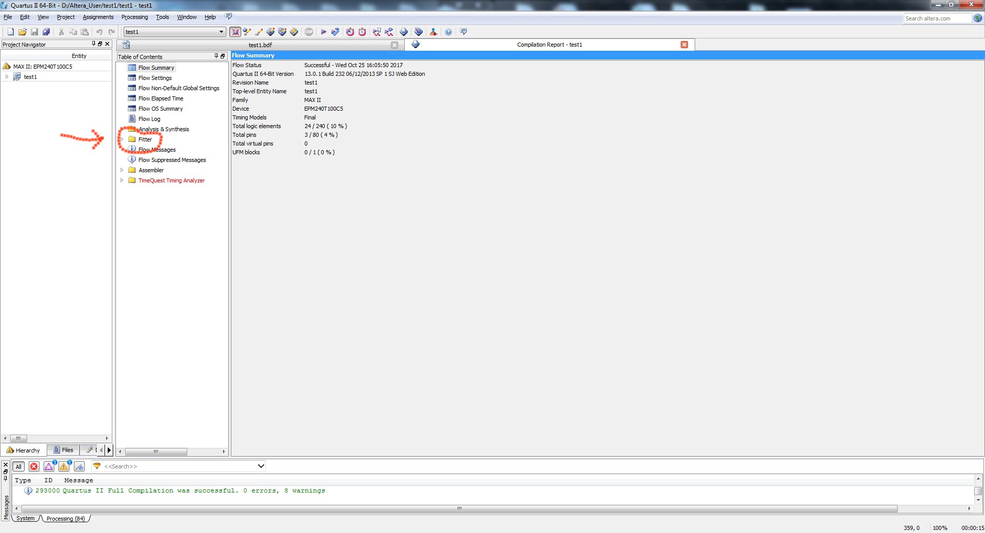
Now close the "Pin Planner" (no need to save anything here) and return to the main environment. From here compile the project again:

and check that all pins are set up as required. To do that go, soon after the compilation, click on the "Fitter" folder:
and then clock on the "Resource selection" folder:
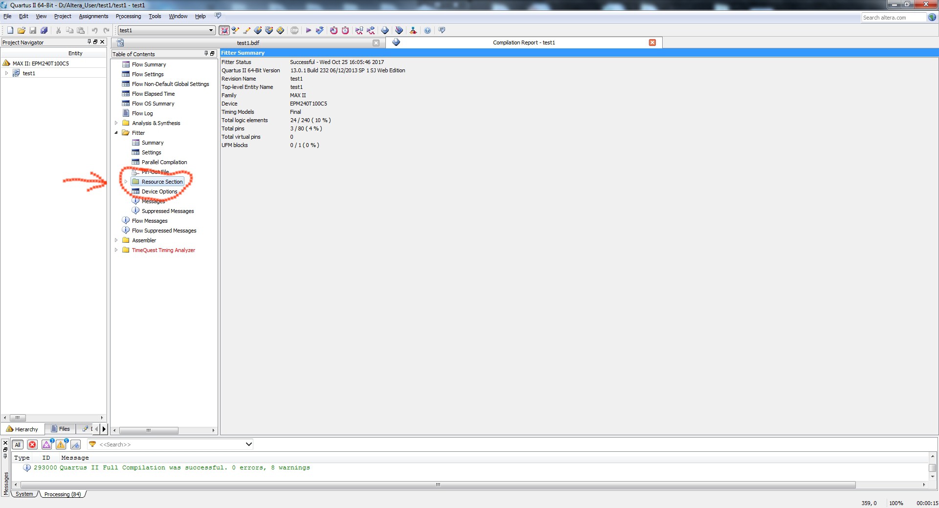
and on the "All Package Pins" element:

and check that all the pins are configured as wanted.
USB Blaster connection procedure
After that you are ready to upload the configuration into the CPLD.
To do that you must follow the suggested steps as described in the Usb Blaster User Guide:
- Check that the target (the CPLD Fun Board) is not powered;
- Connect the Usb-Blaster programmer first to the Workstation USB;
- Connect the JTAG cable to the target;
- Power the target. This means connect the CPLD Fun Board USB connector to an other USB port on the Workstation.
Remember that the USB Blaster can't power the target. The power comes from the USB connector.
Here a short video about how to connect the USB Blaster dongle:
CPLD programming (Quartus II)
Now click to the "Programmer" icon in the main window:
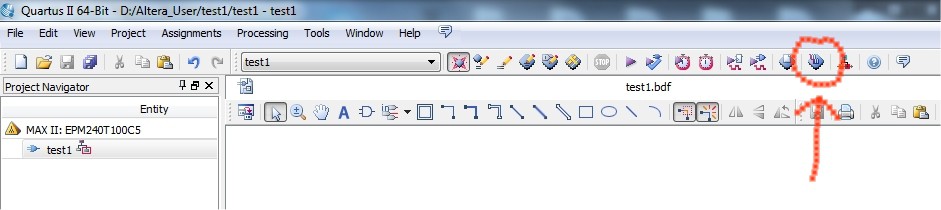
and the "Programmer" window will pup up:
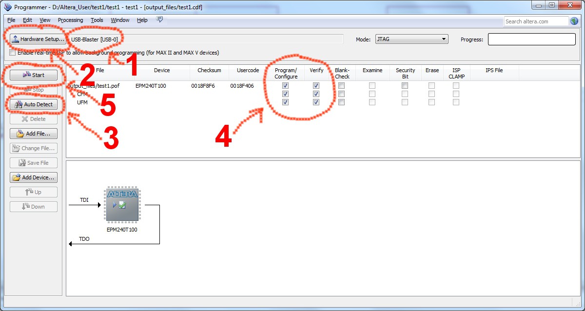
Now some check:
- Check if the "USB-Blaster" device is selected (1);
- If not, press the "Hardware Setup..." button and select it (2);
- Press the "Auto Detect" and you shouldn't see any error (3);
- Check all the "Program/Configure and "Verify" check boxes (4);
- Press the "Start" button to upload (5).
STM32 clock generation sketch (Arduino IDE)
Now you must upload a "Sketch" in the STM32 with the Arduino IDE to generate the needed clock signal.
Copy the following code to a new sketch inside Arduino IDE:
void setup() {
  // put your setup code here, to run once:

  // Set the MCO pin to output the clock to the CPLD (GCLK1 pin 14). See STM32F103 Reference Manual RM0008
  RCC_BASE->CFGR =  RCC_BASE->CFGR | 0x07000000;    // Set MCO[2:0] = 111 (inside RCC_CFGR register) for 36MHz clock output
  GPIOA->regs->CRH = GPIOA->regs->CRH | 0x00000003; // Set output mode on PA8 @ max freq 50MHz (MODE8[1:0] = 11)
  GPIOA->regs->CRH = GPIOA->regs->CRH & 0xFFFFFFF3; // Set output mode on PA8 as general push-pull output (cnf8[1:0] = 00)
  GPIOA->regs->CRH = GPIOA->regs->CRH | 0x00000008; // Set output mode on PA8 as alternate push-pull output (cnf8[1:0] = 10)

}

void loop() {
  // put your main code here, to run repeatedly:

}
and upload it, but before check that the target board is a "Maple Mini" running at "72 MHz" and having a the "Bootloader 2.0":
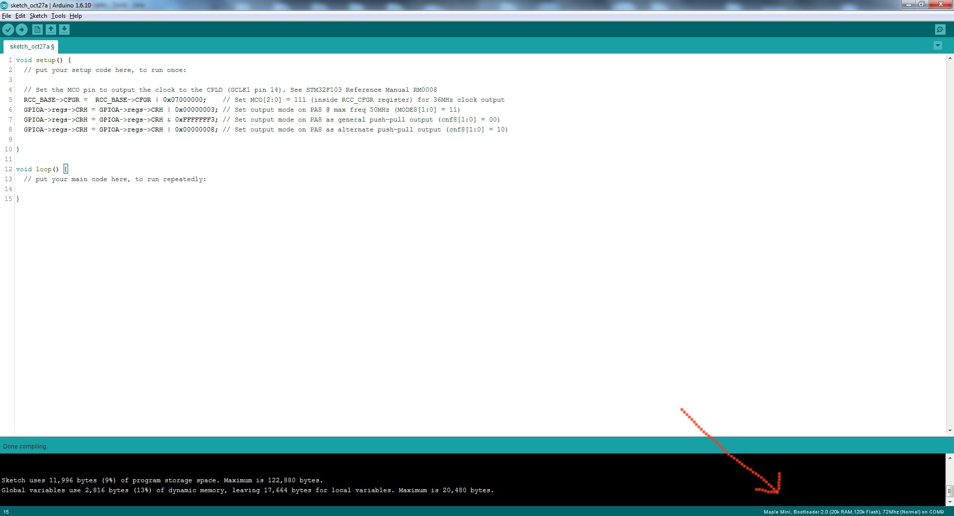
After the upload LED1 will blink at about 2Hz. If not check that the DEV_OE led is off; if it is on turn it off using the DEV_OE switch.
Here is the result:
In the video you can see that when the RST button is pressed and the STM32 resets, the blink stop for a while. This because the clock is provided by the STM32.
You can see the effect of the DEV_CLRn button that reset all the FFs inside the CPLD making the counter stop. Same behavior pressing the USR4 button connected with the Clear signal of all configured counters.
Switching the DEV_OE all the CPLD I/O pin go in HiZ, so no blinking again.
Of course the DEV_CLRn and DEV_OE have effect only if you have previously checked them in the Quartus II setting windows.
USB Blaster disconnection procedure
Now, to disconnect the USB Blaster dongle you must follow the suggested steps as described in the Usb Blaster User Guide:
- Power off the target. This means disconnect the CPLD Fun Board USB cable;
- Disconnect the JTAG cable from the target;
- Disconnect the Usb-Blaster programmer from the Workstation USB.
Here a short video about how to disconnect the USB Blaster dongle:
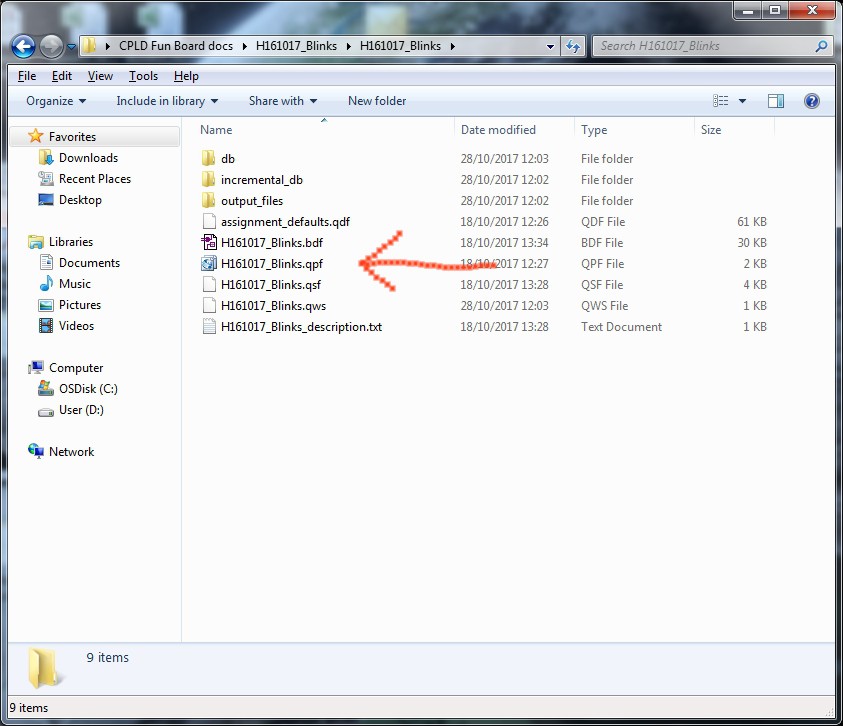
An example ready to use
I've made a blink example ready to use. In this example it is used the schematic editor, but note that this is not the best way to use this devices (the right way is to use VHDL/Verilog languages...). Download the file H161017_Blinks.zip (the file is too big for this site, so it's stored externally) and unzip it taking its directory structure. This is a complete Quartus II project, so you can open it from the main menu with "File" -> "Open Project..." selecting the file .qpf inside the downloaded zip file:
It is a blink led example similar to the previous, but with an other series of divider connected to the optional 50MHz oscillator. If populated it will blink the LED2 too:
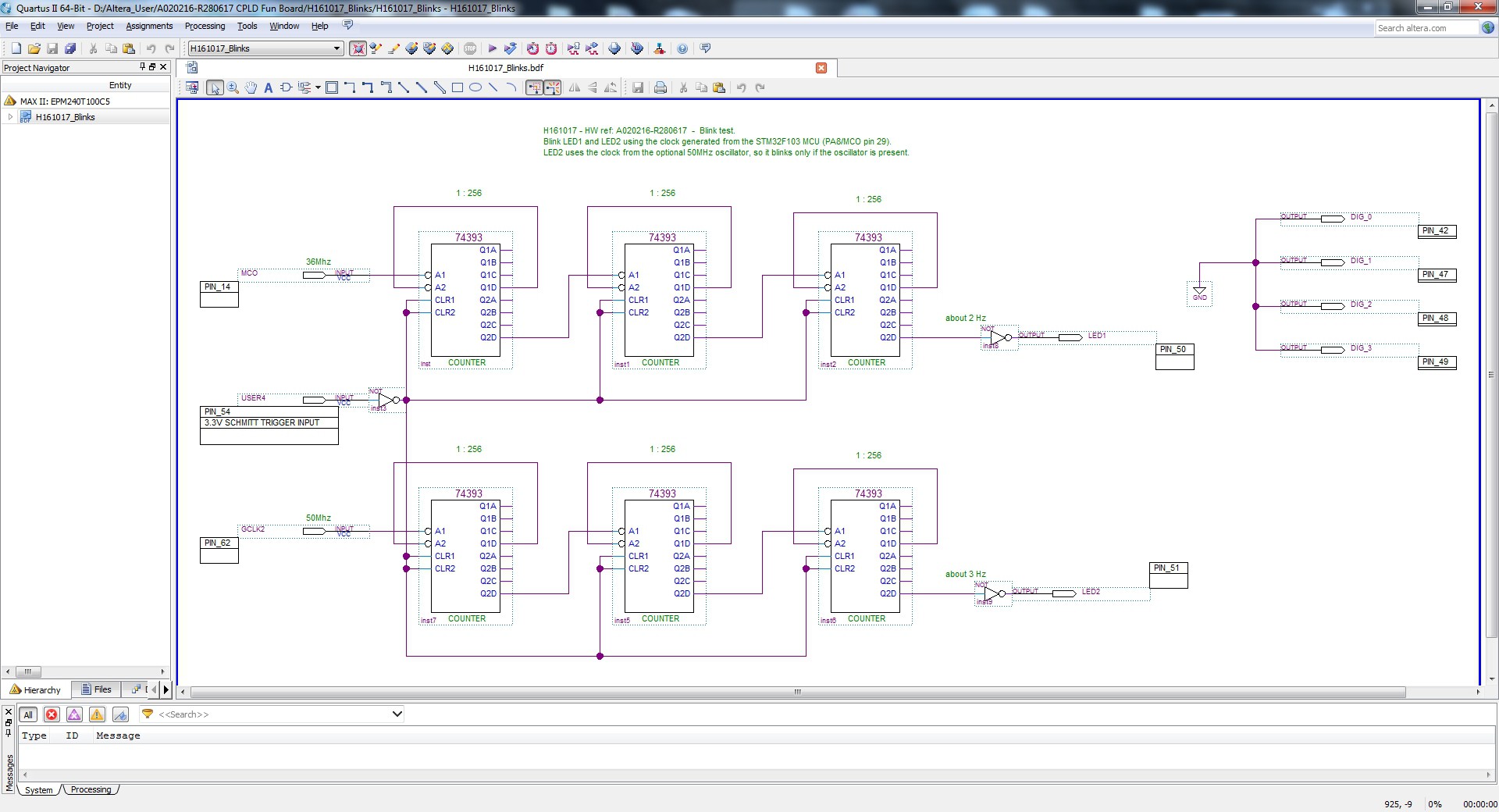
More, the four outputs (DIG_0-3) that drive the common pin of the four digit of the 7-segment on-board led display (see the schematic) are tied to GND to avoid the flow of a low drive current from the internal pull-up resistors due to the default configuration for all the unused I/O pins (HiZ with pull-ups enabled). This current is the cause of the very low light that you can see from the led display in the previous CPLD configuration.
Remember to verify always the "general device pin options":
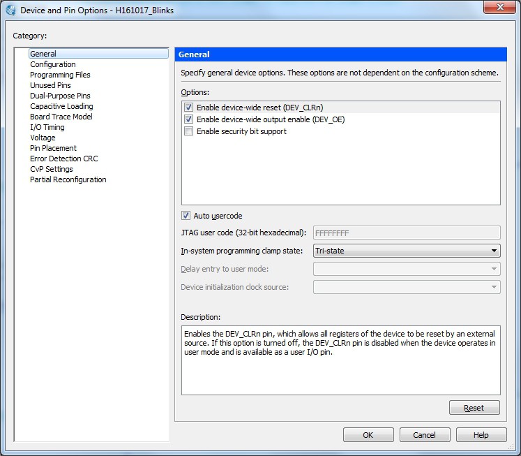
and the "unused pins" option:
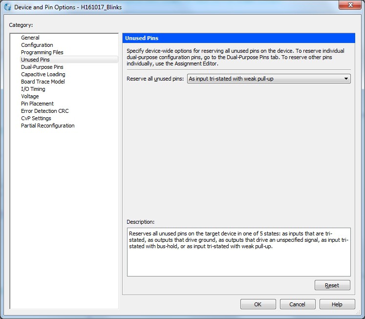
as described in the previous example, and in general all the others settings.
The sketch to use for the STM32 is in the "File" section: S161017_BlinkTest.ino.
This sketch will generate the 36MHz clock to blink LED1, and will blink the LED_PB1 led connect to the STM32 too (see inside the code of the sketch).
The following video shows the result:
Both the boards have the same CPLD configuration and the same sketch on the STM32 MCU.
The board on the right (it is a previous PCB revision) has the 50MHz oscillator populated.
You can see that pressing the RST button (STM32 reset) the LED1 stops to blink for a while because the STM32 stops to generate the clock, but LED2 on the right board continues to blink because the clock comes from to the 50MHz optional oscillation (see the schematic).
The DEV_CLRn button stops both LED1 and LED2 blinking because forces all the FFs of all the LEs (Logic Elements) inside the CPLD to reset (until it is released), instead the LED_PB1 is unaffected because driven by the MCU.
Discussions
Become a Hackaday.io Member
Create an account to leave a comment. Already have an account? Log In.