 Just4Fun
This is a ready to use example of a custom "multi-functional" controller for a 4 digits 7-segments led display (single segment "graphic" drive mode with digits multiplexing), plus 4 status leds, plus 4 push buttons, using a bidirectional data bus (DATA_0-7) and a register selection bus (SEL_0-2). The command signals are an active low write signal (WR_EN) and an active low read signal (RD_EN). The behavior is very similar to a SRAM device.
To make things easier, in this example it is used the schematic editor and the 7400 devices family library, but note that this is not the best way to use a CPLD (the right way is to use VHDL/Verilog languages...).
The schematic is the following (it is better use the Quartus II schematic editor to view it, opening the project):
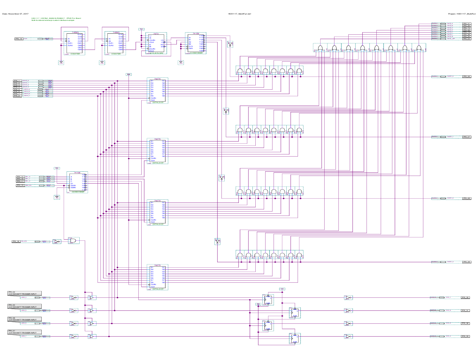
The design is similar to the previous example. The input clock for the multiplex comes from the 36MHz clock (from the STM32 MCU), and is divided by two 1:256 dividers (74393).
The internal digit registers are now 8 bits wide, because now each single segment can be controlled (plus the "dot"), and there is a 4 bits register for the four leds LED1-4.
Only DATA_0-3 lines are really bidirectional, DATA_4-7 lines are not used in "read" mode and are tied to "1" using internal pull-up resistors.
A logic "1" in the DATA bits means "led turned on" or "push button pressed".
The "registers map" valid for the write operation is ("Reserved" means here "not used"):
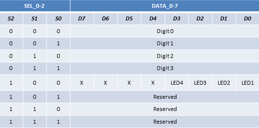
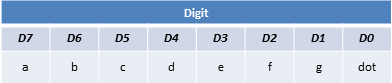
where the generic "Digit n" byte used to turn on or off each single segment, is defined as:
This one is for the read operation (to check the four USR4-7 buttons status):
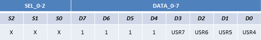
In the "read" mode there is no real register involved, so the SEL_0-2 lines are all "don't care".
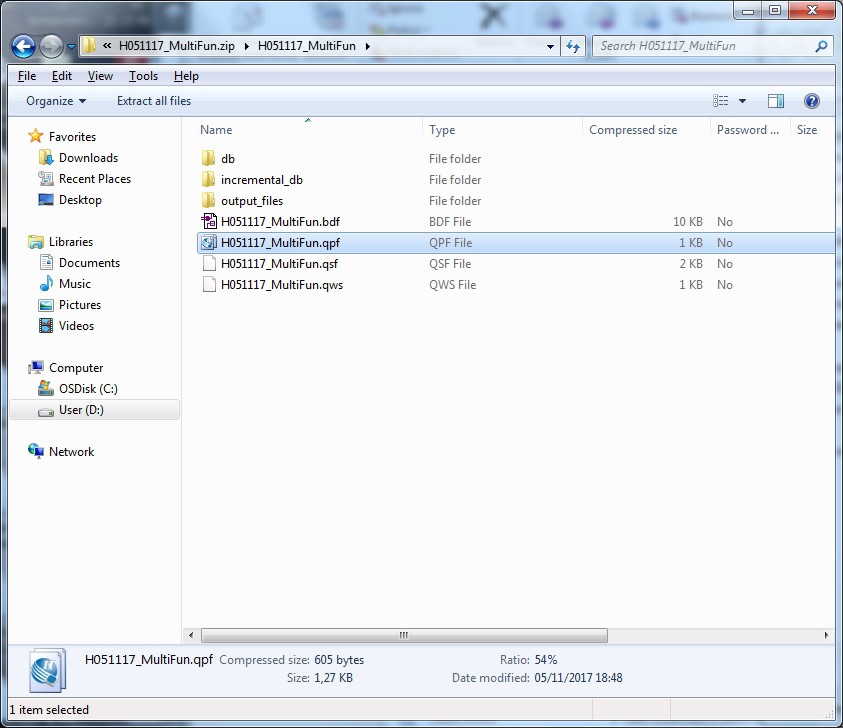
The complete Quartus II project can be downloaded from this file: H051117_MultiFun.zip (the file is too big for this site, so it's stored externally).
Unzip it taking its directory structure, and open it from the main Quartus II menu with "File" -> "Open Project..." selecting the file .qpf:
Upload the configuration into the CPLD as described in the Log: "Blink led example. Step by step guide".
WARNING: Because this is a bidirectional interface, take in account the considerations done in the "The DEV_OE switch and led" Log.
The sketch for the MCU side is S051117_MultiFun.ino (in the "Files" section) and must be uploaded using the Arduino IDE to run an application example.
The result is shown in this short video:
The USR1-3 and BUT buttons are managed directly by the MCU.
Discussions
Become a Hackaday.io Member
Create an account to leave a comment. Already have an account? Log In.