 Vlad Ivanov
While the boards and the mechanic components are being delivered I thought I'd make an overview of the planned FPGA design stuff.
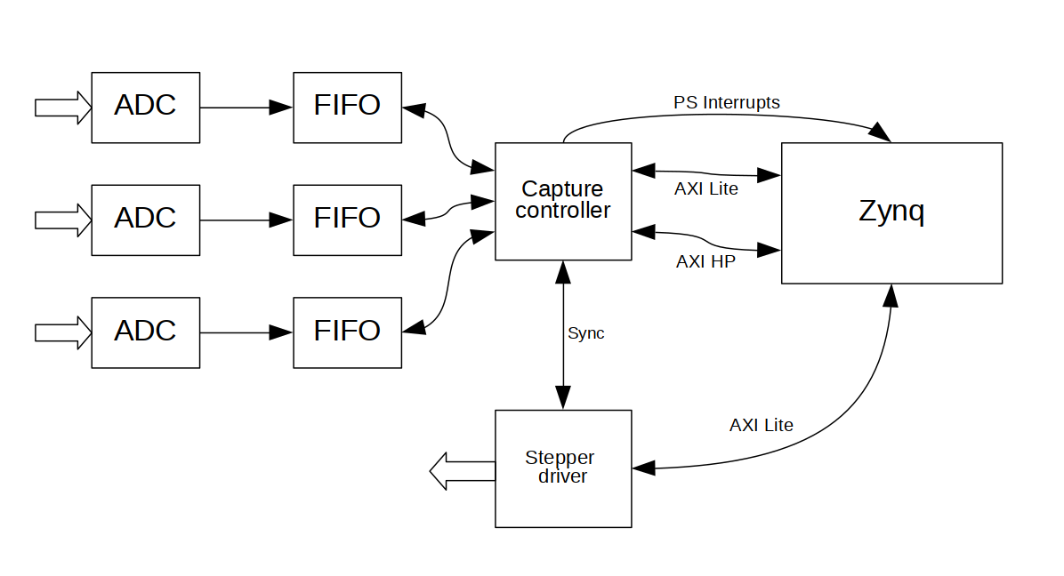 On this diagram, Zynq refers to the Processing System block inside the SoC. As you can see, there are three ADCs, which output 12-bit samples. Samples from each one of them are stored in a small FIFO buffer. The capture controller module scans each FIFO periodically and, once there is enough data, submits a number of transfers through AXI HP interface. Using FIFOs allows us to account for system bus availability and also to store data in bursts, which is faster, especially on some low-budget Zynq boards.
Finally, the AXI Lite interface for both of these blocks is needed to actually interact with the software through the register interface. And while we're at it and have an FPGA, the stepper driver can also be put in the programmable logic.
Discussions
Become a Hackaday.io Member
Create an account to leave a comment. Already have an account? Log In.