 Yann Guidon / YGDES
In a previous log, I sketched a different approach to handle the CALL instruction.
The current datapath draws inspiration from the YASEP and it looks like this on the main YGREC diagram (only a close-up):
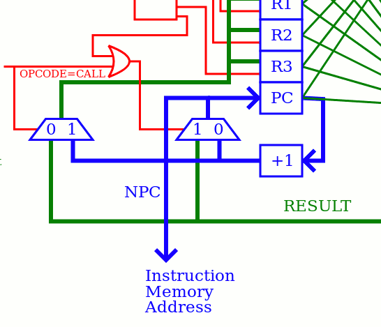
One pair of MUX2 (controlled by almost the same signal) swap the RESULT bus with the value of PC+1.
- The usual ALU operations get the operands from the register set, go through the ALU, and the result is written back to the register set.
- The NextPC (or PC+1) value is generated from PC and goes back to the PC (and to the memory address bus).
- When CALL is executed, the inputs of the register set and PC are swapped with a pair of MUX.
This is a structure I introduced in the YASEP and carried over to the YGREC, with confidence because it seemed to work well. But this structure sits like a Sphynx at the end of the critical datapath and costs a precious MUX2 delay that I want to optimise out. The previous related log is first dent into the old design.
The latest design removes this bottleneck, by actually moving it away from the critical datapath and narrowing the selected values to those that make sense.
- PC can get written with PC+1 or the end of the SRI selector, because this is the field that indicates the destination of a jump. This leave more time to fetch the next instruction, compared to going through the whole datapath and the final MUX. Slower memories can be used.
- The value of PC+1 gets inserted in the datapath earlier, in a source selection MUX where there is less timing pressure. The destination register is given by the SND field of the instruction so the next PC can be inserted near the ROP2 unit for example, with a sort of "pass" function. This puts more pressure on the other MUX2s which require a more complex bypass signal though...
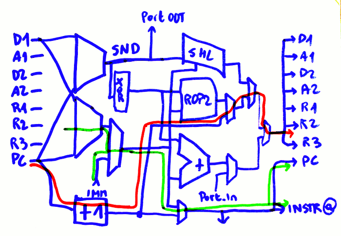
The above diagram shows the flow of data during the CALL instruction. The red path shows the updated PC being written to the register set while the SRI bus is written to PC. The final MUX tree will be adjusted when the latency of each unit is well characterised.
No more MUX2 ! In the ProASIC3 this saves maybe 1ns in the instruction cycle time...
PS: The only thing to avoid is a conditional CALL or write to PC because if it does not get executed, the write to PC is inhibited. Which will stall the program because the next instruction is not fetched ! So if a "not taken" CALLl is executed, a second cycle must be issued. Remember : otherwise, only the LDCx instructions can inhibit the write to PC !
Or better: the PC MUX is reversed back to PC+1 by the condition. The pseudocode would read something like:
NPC <= SRI when (condition=true) and (opcode=CALL or (opcode=SET and AddrSND=PC)) else PC1;
Since the value of SRI takes about 5 logic gates to compute, there is enough "time" to check the condition (MUX4+XOR: 3 gates deep) and the opcode (2 gates). The core can run fast with a semi-parallel, overlapping fetch of the next instruction memory and this covers the SET and CALL opcodes, with Imm8, Imm3 or register with condition.
Unfortunately the other jump methods (like IN, or computed jumps) are not possible anymore and the ISA orthogonality is broken :-( everything must go through a temporary register, which consumes another instruction and cycle. Short loops can't be done anymore :
R1 = 42 ; block size

;; block copy :
SET D2 D1 ; copy data
ADD A1 1  ; update the pointers
ADD A2 1
ADD R1 -1  ; decrement the counter
ADD PC -4 IFZ  ; conditional loop back
without the last instruction, a temporary register is required to hold the target address and the number of available registers is already very small...
Note that this problem appears mostly on semiconductor-based implementations where each MUX2 adds latency. The ALU/SHL/ROP2 units in relay technology will still add some latency as well anyway. But fetching the next instruction will always take "some time" too.
The most suitable solution seems to be to add a "negative delay bypass" (another MUX2) and a "wait state", a one-cycle inhibition of the PC update, so a taken branch will use two cycles instead of one.
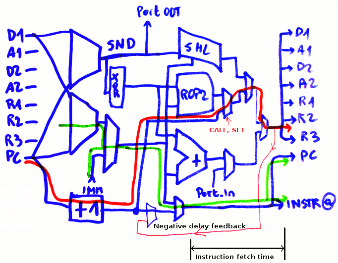
So far, PC update is inhibited under these conditions:
- core is in pause/debug/halt
- LDCx's first cycle (where the program memory address bus is fed with the SRI value)
- Writes to PC (other than SET and CALL) where condition is true
This one cycle delay for taken branches is a good compromise because it doesn't add much complexity to the core and lets all the other instructions run faster (and/or consume less power, to be determined).
Now I'll have to find how to tell the FPGA that certain signals must not be counted in the critical datapath.
Discussions
Become a Hackaday.io Member
Create an account to leave a comment. Already have an account? Log In.
Another aspect to remember : with only 8 bits for instruction addresses, there is almost no need for relative addressing of instructions. Short displacements from -4 to +4 have the advantage of using only one instruction. For longer jumps, an immediate value is more convenient. Code of this size (256 instructions) is not going to be dynamically relocated (the program is in EEPROM or other non volatile storage) and addresses can be fixed at assembly time. So unlike x86 and the other 8-bits or 16-bits architectures there is little need for powerful relative jumps. Short relative jumps however are critical to skip over a few instructions such as long immediate jumps.
Overall these tricks keep the number of opcodes very low and decoding is almost straight-forward :-)
Are you sure? yes | no
Yann, if I understand your design correctly, the negative delay is needed for compensation of the delay for PC+1 .
For relative jumps, you could add the displacement to PC instead of PC+1, so you dont need the +1 block in that case.
Are you sure? yes | no
I agree on some of your assertions : I have considered replacing the PC incrementer with a full adder.
However :
1) this increases the gates count, and duplicates the ADD unit
2) this increases the latency : PC+1 is neatly just as fast as the MUX8 that reads the operands. Using a full adder will break this convenient balance.
3) this works for unconditional relative jumps, but for the conditional jumps, two alternate values are needed at the same time : the following instruction, or the new branch. They get MUXed just after, when the condition code is finally available. But if you want a conditional relative jump without two parallel units (inc and add), you must MUX between PC and the displacement, which totally bloats the latency (the usual compromise : latency vs parallelism, you can't have everything, it's the old A×T² design rule).
In the end, delay is unavoidable, but I have pushed it to where it is not disturbing anything unrelated.
The remedy I have found adds a MUX2 row (8 gates + some decoding) and another condition for inhibition of PC increment. The other instructions work at full efficiency :-)
Are you sure? yes | no
I ment that PC + immediate could be done in the adder that is below the ROP2 in your last drawing. The +1 block stays in place for normal PC increment.
I do not know where your condition code comes from, and why it can not be available in time.
Are you sure? yes | no
oh, sorry, I misinterpreted your reply :-) I might have been biased by my own thinking...
if the main adder is used, then the datapath has no time left to fetch the next instruction (memory has latency too). In this design (aimed at A3P FPGA), the next instruction is prefetched while the current one executes, so the next address must be known sufficiently in advance.
So the added mux (look at my updated diagram) helps add some delay while PC is inhibited from updating during one cycle. The computed result (or anything coming from anywhere) has time to settle, during the 2nd cycle, and the memory can read the target instruction in time.
Are you sure? yes | no
Ok, I did not realize that the new PC should already be used to get the next instruction in the same cycle. I wish you success with the following design steps...
Are you sure? yes | no
@roelh : yes it was not obvious from the previous diagrams.
I use design rules that are reasonably compatible between relays and FPGA : one FPGA gate is approx. 1ns latency each, and the RAM lookup takes approx. 3 or 4ns, which is about 4 gates. The A3P's RAM blocks have latches at the output so they require the address to be present 4ns before the output is updated (at the same time as the PC register).
Similarly, the relay program memory has latency because the address signals must be amplified a lot, so 3 or 4 relays of latency is a reasonable estimate, and the output is latched as well.
Thus I can develop a structure that is compatible with both technologies (and probably more) :-)
Are you sure? yes | no