 Yann Guidon / YGDES
Note: this log is obsoleted by Bitslice
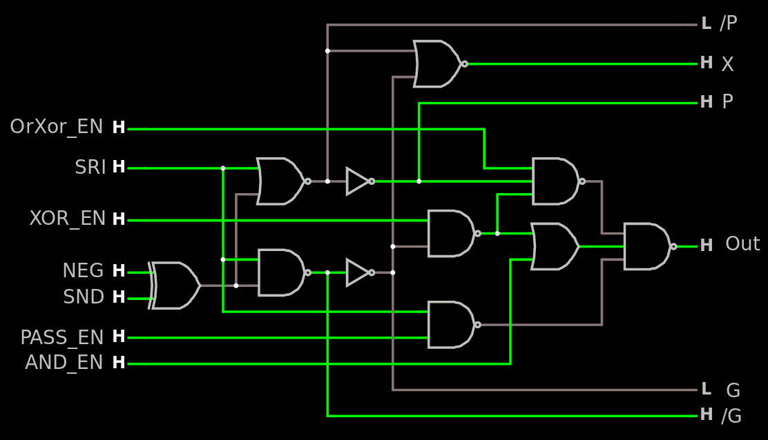
After the last log Adder with Falstad, I also converted the ROP2 bitslice to the interactive simulator :
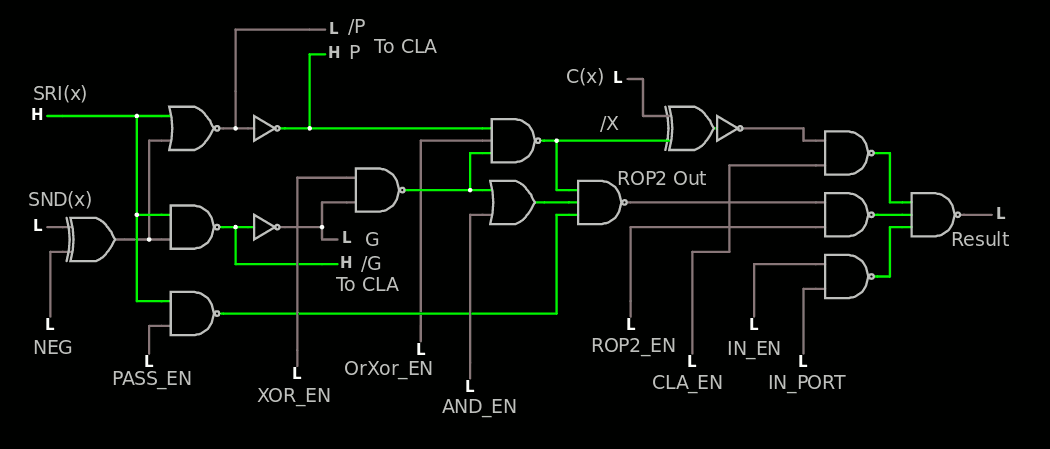
There is still the challenge to disable the output of the CLA so it can be combined by ORs with the rest of the units.
My guess was to decompose the end XOR and include the "enable" signal at the end of the combining gate but I get the wrong polarity. Instead I have this solution for XA1:
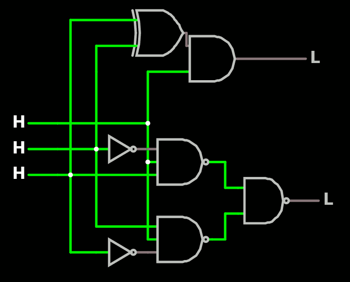
however the fanout for the "enable" signal is doubled and this feeds 2 gates with 3 inputs, which uses more space...
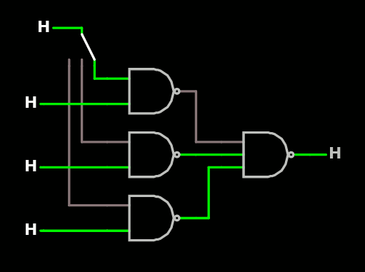
It's hard to reduce the XOR gate and each technology has their own tricks up their sleeve to implement it, so I prefer to keep the XOR as is and the output is MUXed with a classic 2-levels NAND circuit:
Now I have moved the final XOR of the CLA back into the ROP2 circuit, which also saves one gate because I duplicated a (N)OR. The final XOR is driven by the "shared XOR" which has a reverse polarity so you can see I added an INV but it can be bubble-pushed in the CLA or in the final MUX as needed. Source:
The truth table is updated :
      NEG  PASS_en AND_en XOR_en OrXor_en ROP_en CLA_en IN_en
/OR   0      x      x      0       1      1       0      0
\OR   0      x      0      x       1      1       0      0
XOR   0      0      1      1       1      1       0      0
AND   0      0      0      1       0      1       0      0
ANDN  1      0      0      1       0      1       0      0
SUB   1      x      x      1       1      0       1      0
ADD   0      x      x      1       1      0       1      0
PASS  x      1      x      x       0      1       0      0
IN    x      x      x      x       x      0       0      1
clear x      0      0      0       0      0       0      0
Simulation with Falstad helped uncover some non-trivial "don't care" states.
The PASS code is back to "ROP2 land" but this shouldn't create too many problems in the decoder.
I added the IN instruction and left the SH codes for a future version, so it fits with the final NAND3 gate.
Some signals such as AND_en are updated because the ROP2_en "shadows" them.
It seems XOR_en and AND_en could have their names swapped ? AND_en is 1 only for XOR, and XOR_en is 0 only for OR...
Discussions
Become a Hackaday.io Member
Create an account to leave a comment. Already have an account? Log In.