 Yann Guidon / YGDES
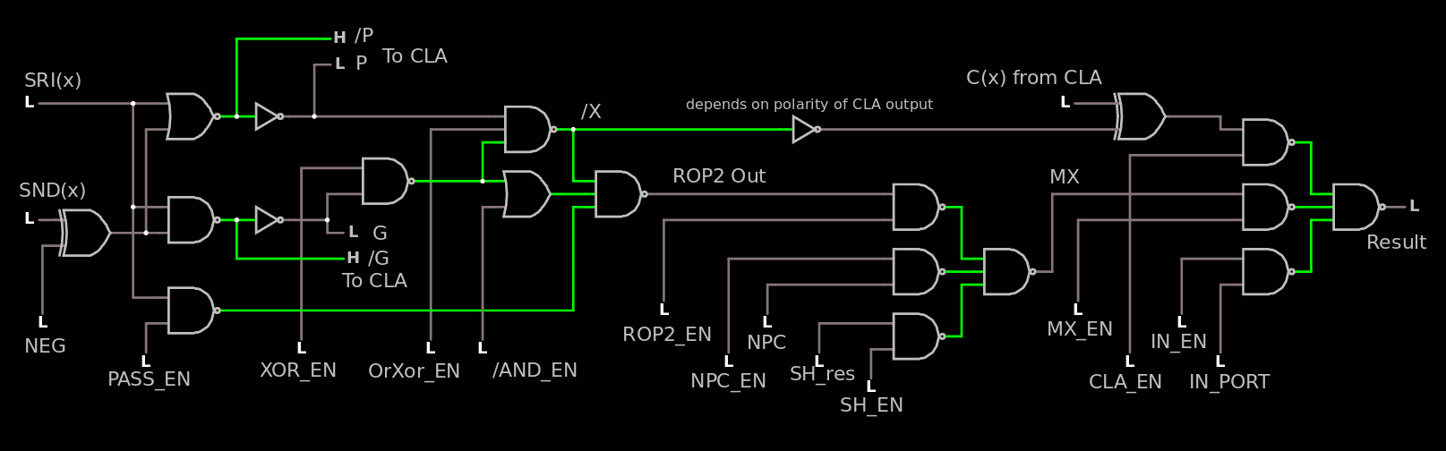
The ROP2 and ALU part has been slowly expanding to the SUXEN but the log 70. The nexus reminds that something is missing : I have forgotten to include PC+1 (NPC) value. So another level of MUX is required, which is fortunate because I had also left the SHL result. I can then use another full MUX3.
In a previous log ROP2 with Falstad I came up with this diagram:
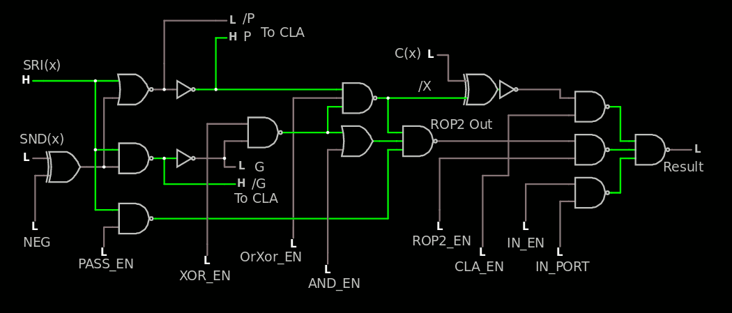
and it seems it must be extended a bit with another layer of MUX3 (source)
The CDP of the whole stack is about 10 simple gates and I have not counted the CLA or the IN port.
It's pretty satisfying to see that whole "datapath" in one picture, at last :-)
You can see a lonely inverter on the /X signal. This is an optional correction for the output polarity of the CLA. It can be omitted if needed, it's on the "slow path" and provides some degrees of freedom for the CLA design.
Speaking of slow paths : there is one OR just before the ROP2_out signal but it looks uncompressible and not critical so I leave it here. The input XOR for SND is critical though. I'll see how I can reduce the output XOR from CLA, there is a fun trick to play with BJT ("enable" by playing with the CLA_EN signal tied to the pull-up resistor of the interlocked pair).
Total gates : 20, 13 NANDx 2 XOR, 3 INV, 1 OR, 1 NOR.
That's 160 gates for the 8-bits datapath (ignoring the CLA and SH circuits). It looks pretty easy to layout and route but the output and the inputs will be located at the same side to ease routing of the register set. I'll probably move to a 3-tiles high organisation for FPGA & ASIC.
Update :
I might have found a trick to save a bit of stuff somewhere :-)
The idea is to combine NEG and PASS_EN at the XOR input level, which saves one NAND2 and reduces the NAND3 to NAND2 (which can also add one more input in the datapath if needed). There is a need however to get /L somehow/somewhere but a XOR contains 2 inverters anyway. But NEG and PASS_EN can be controlled at the decoder level and the other inverter is moved/shared.
Oh and I also replaced the OR (for AND_EN) with a NAND2, one input has an inverter while the other input can be inverted at the decode level. (source)
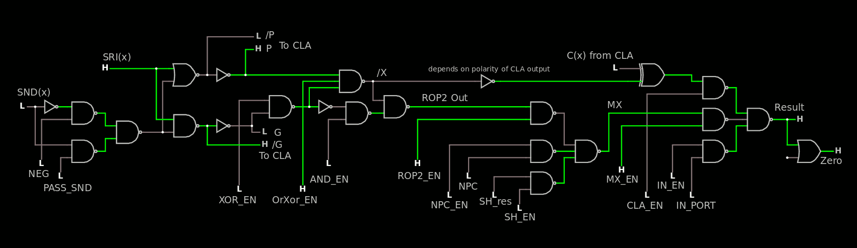
PASS_EN is renamed to PASS_SND because it makes more sense.
I have also added the Zero detection. That would be a OR8 (in a way or another).
Here we see the signal going from SRI to the Result output, NEG and PASS_SND are disabled so the value flows through the OR logic : OrXor_en, ROP2_en, MX_en are enabled.
In the decoder's logic, AND_EN, NEG and PASS_SND are affected. This removes several "don't care" situations.
     NEG PASS_SND AND_en XOR_en OrXor_en ROP_en CLA_en IN_en MX_en
OR    0      1      0      0       1      1       0      0      1
XOR   0      1      0      1       1      1       0      0      1
AND   0      1      1      1       0      1       0      0      1
ANDN  1      0      1      1       0      1       0      0      1
SUB   1      0      x      1       1      0       1      0      0
ADD   0      1      x      1       1      0       1      0      0
PASS  0      0      x      x       1      1       0      0      1
IN    x      x      x      x       x      x       0      1      0
clear x      x      x      x       x      x       0      0      0
.
Discussions
Become a Hackaday.io Member
Create an account to leave a comment. Already have an account? Log In.