 Yann Guidon / YGDES
Things are looking good on the front of hexadecimal display. #Numitron Hexadecimal display module will soon get its first PCB module so it's time to think about how it will be used.
@llo offered to help with the project so I created a couple of diagrams. The first shows the general organisation of the YGREC computer (either 8 or 16 bits version) and how the displays and the assembler/disassembler are used to program, step into code, examine and inspect the processor and the sytem :
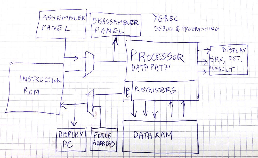
In an ideal, hypothetical computer, the middle parts (with the MUXes) are removed. The instruction bus is connected directly to the processor and the PC is tied to the instruction ROM address bus.
The system is "cut in half" to greatly enhance the manufacturability/testing, but also the design of the software and the hardware. These boards allow us to inject signals to probe into the processor.
For example if you want to read the value of a given register : switch the assembler panel on, change the SRC knob to the desired register, and directly observe the value displayed by the SRC display from the processor.
There are at least 5 digital displays and these should be sufficient for programming and troubleshooting:
- immediate data on the disassembler panel
- current instruction address
- SRC operand
- DST operand
- RESULT value
So on YGREC8 that's 10 hex digits, and 20 for YGREC16. I don't count the status flags (Zero, Carry, Sign).
(now I'm waiting for @llo to make a clean version of the diagram ;-) )
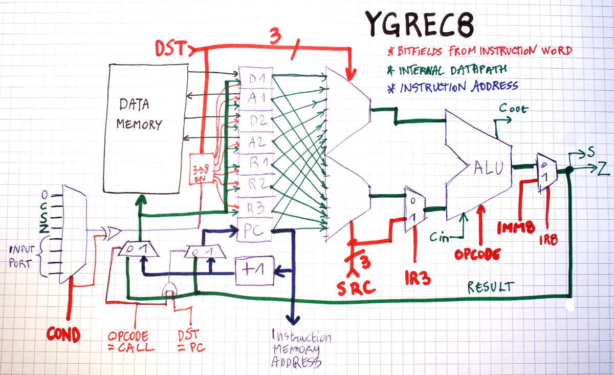
It was also time to upload the diagram of the processor's datapath. Here is the first draft, almost complete. It misses a few details but you have the most critical features right under your eyes:
I'm hoping to get a proper, clean, computer version (SVG or PNG) "shortly" :-)
The datapath is pretty straight-forward : two operands are read from the registers, two immediate fields are injected (before and after the ALU) and the result is looped back to the register set.
There is a little magic trick with PC to allow function calls : if OPCODE=CALL the destinations are swapped and the next PC is saved in a given register instead of PC. The computed address from RESULT is loaded into PC instead of the other registers, which implements a sort of Jump.
Data memory is almost like the YGREC16 but with only 2 ports. I think the relay version will have maybe 64 bytes of DRAM only, to keep the system small and gain experience for the YGREC16 without using too many parts.
You can see how conditions are managed : it's a simple MUX8. One input is constant (for NEVER and ALWAYS), there are the 3 usual status flags (Carry, Sign and Zero) and additional inputs, that can come from outside signals (à la /EF1-/EF4 of the CDP1802). The 4 signals makes it easy to communicate with outside hardware, sensors, users...
Now is the time to work on the assembler and disassembler panels.
20171113 : the above diagram has a major flaw with the Imm8 MUX2 :(
Discussions
Become a Hackaday.io Member
Create an account to leave a comment. Already have an account? Log In.