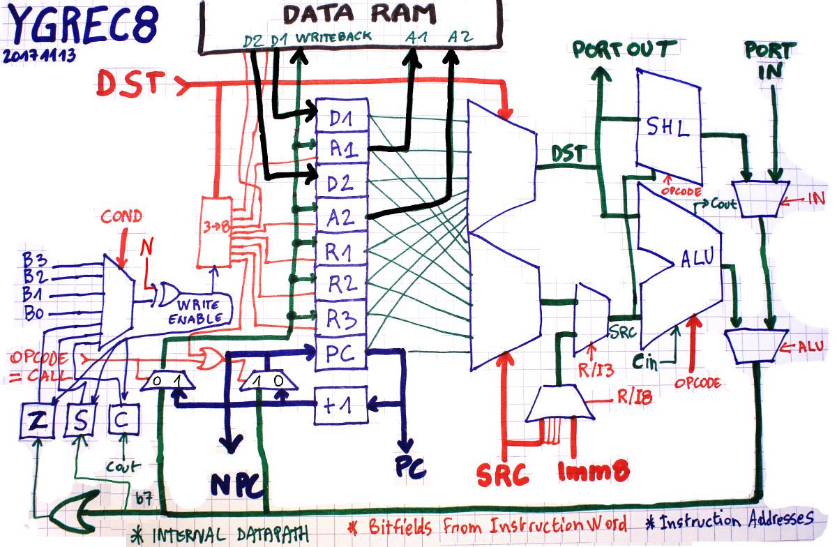
I found that I made a few errors in my precedent diagram and I have updated several aspects. Here is only an early draft, until @llo makes a vector version.

- The Imm8 field is now integrated at the right stage of the datapath.
- I/O ports are also integrated, according to the latest developments.
- The Z/S/C flags now have their own write-enabled registers.
- NPC appeared, because the A3P SRAM blocks have their own latches already. It might also be useful for debug.
- The R/I3 condition is not right, it should be : R/I8 or (R/I3 and /R/I8)
- I added the SHL unit
- D1 and D2 are now explicitly outside of the core, stored in the SRAMblock buffers.
The condition block on the left is not well laid out but hopefully @llo will make it better :-D
Back to VHDL now...
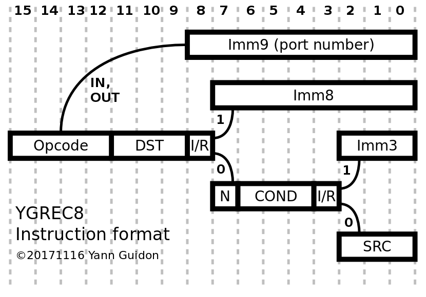
And I updated the instruction format diagram :

yup the condition Negation flag has moved... I don't know why. But it's coherent with the VHDL code.
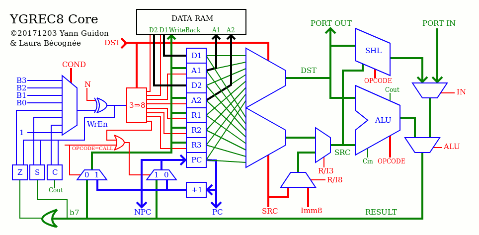
20171203 : I got a stable and nice diagram of the core !

 Yann Guidon / YGDES
Discussions
Become a Hackaday.io Member
Create an account to leave a comment. Already have an account? Log In.