 Yann Guidon / YGDES
A previous log 16. Inspect and control the core has shown the high level view of the debugging system. Here we see how it is implemented for a SPI interface, such as a Raspberry Pi.
The necessary signals are
- MOSI : data sent to the YGREC8 core
- MISO : data received from the YGREC8 core
- SCLK : synchronous clock
- Select : control which chain is accessed.
The protocol is half-duplex to prevent incoherency. This means that MOSI and MISO could share a bidirectional pin:
- Select=low : YGREC8 core receives data
- Select=high : YGREC8 sends data
So the physical interface could use 3 or 4 pins, depending on the requirements. The interface is easy to bit-bang with a microcontroller or something else.
The transitions of Select reset the appropriate chains. For example, when Select=low, the sending circuits are in RESET mode. The Receive informations will only become active and registered when Select goes high (so Select is also a clock input to the DFF of certain internal registers). The Select pin can be left with a weak pull-down, as well as the data pin and the clock pin. Any number of clock cycles has no effect, as long as Select remains low (the debug controller can then flush the shift register by sending 0s, then its own 32 bits).
Note : the design is aimed at simplicity and compactness, using the least possible gates.
When Select=low, the core is in receive mode.
There is a 32-bits shift register that shifts bits in. Any number of clock cycles can be sent, only the most recent bits are considered. The bits are described in the log 16. but here they are again :
- 16 bits for the CONTROL register, with the bits RESET, BYPASS, UPDATE, START, STOP, STEP, as well as bank select to access the breakpoint & profiling registers.
- 16 bits of INSTRUCTION, which can be sent to the core, or eventually later to the breakpoint & profiling registers.
When the Select pin goes high, the shift register is transferred to the appropriate registers, depending on the state of the bits of the control register. For example, if the "Instruction Bypass" bit is set, the core will execute the 16 bits of instruction that are provided in the currently written word.
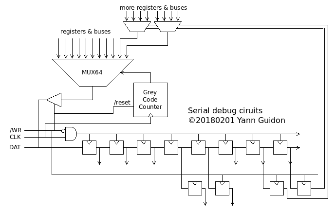
Physically, the circuit is just a string of 32 DFF, with a common clock that is gated by the Select signal. No reset is needed (except a few sensitive signals). The Select signal will latch the appropriate registers and/or update the FSM (after a resynchronisation to the local/internal clock). There are only 32×DFF to drive with the SCLK signal, and fewer for the MOSI signal.
When Select=high, the core is in send mode.
To read meaningful data, the core must have been set to "STOP" or "STEP" state by a previous command.
The circuit serialises 8 bytes, or 64 bits, using a 6-bits counter, which is held in RESET state while Select=low.
Contrary to most SPI interfaces, the data is not serialised with a parallel-in shift register, because of size/cost and timing reasons. Each bit would require a full DFF and a large clock fanout (which is a precious routing resource) as well as a MUX2 (to select between the data and the previous DFF). Timing gets complicated as well.
This is solved by using only (about) one MUX2 per signal, controlled by a Gray code counter. This serialises the 64 bits to the MISO pin, before the counter wraps around (if more than 64 clock pulses are given). Using a large (balanced) MUX also solves the resource problem, as the dedicated clock network is free for the core's use. The Gray code counter prevents glitches, as well as registering the output with a DFF buffer...
20180202:
I hope that it's clearer now :-)
I'm currently working on the MUX64 and Grey code counter.
I must emphasize a few things. First, the priority is to reduce the cell count, and their actual surface, to the minimum, for a ASIC target. This means that only some of the shift register outputs need to be latched again when /WR goes high. Some of these latches can be transparent, as well, because they use 2× fewer transistors.
This subsystem doesn't need to work at very high speed (5MHz ?) so some design rules can be relaxed, for example with fanout. This helps keep the gate/transistor count low. This also saves/avoids the use of a fast clock network. The ANDed clock has a fanout of 32, which is rather high but not a real concern.
The interface is totally asynchronous from the core. This forces us to stop the core while reading the required data. OTOH it would not make sense to read data while the core is running and it saves quite a few DFF and MUX for the read part, as well as a few tricky synchronisation issues. Local resynch will occur at a few places only, where a few critical bits (Start/Step/Stop) will be sampled by the faster internal clock.
/WR and CLK require pull-down resistors on the pins. DAT as well but it's less critical. No global reset is needed. Just make sure you shift in correct data before you rise the /WR pin. Usually it's a RESET command.
Discussions
Become a Hackaday.io Member
Create an account to leave a comment. Already have an account? Log In.
So you have N D-triggers(as a set of registers), which are connected to one MISO wire through controlled switch? And you connect 0, 1, 2...N-1, N trigger one-by-one using counter with Demux on the output? Am I right? Interesting schema.
I think you can speedup this with excluding register number from counter to additional selector register - So you wouldn't have to count from 0 to 63, you can load 8-bit register number to selector and use counter from 0 to 7 for serializing data from register.
As a result you need 16 clockticks for accessing any of 256 potential registers instead of 64 clockticks without selector register.
On the other hand, if you need to read/write all registers in time my schema is not good :)
Are you sure? yes | no
Damnit, I need to draw diagrams :-)
The MISO system is just one way of doing, that is adapted to FPGA and microcontrollers, with few pins.
Higher speeds are possible using more parallel bits, of course, but this is not critical in my application.
The point of the MUX64 is to reuse the "balanced control binary trees" that I design, to reduce the fanout of the control signals. This is an enhancement over the classic MUX trees and classic shift registers, at least for ASICs and ASIC-like FPGAs that I use. The system becomes totally asynchronous, particularly using a Gray code counter to prevent glitches. It solves all the clocking issues I have with other approaches.
There are only 8 bytes in the read bundle and several are selected/addressed by a control word written in the control register.
This is needed to get most of the needed informations about the core's state during debug : in 64 cycles, we have most of the needed informations to update the debugger's display.
Time to draw these diagrams...
Are you sure? yes | no