 Yann Guidon / YGDES
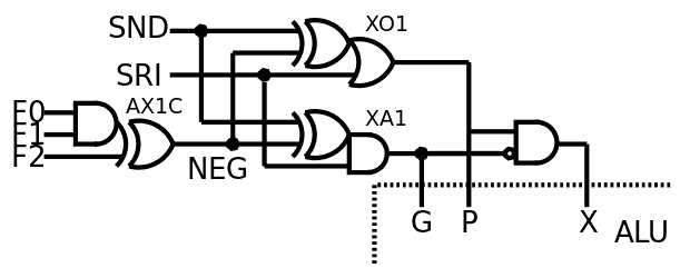
The log An even better ALU touched a few interesting things but has one fatal flaw : the XOR operation needs the NEGated operand SND, because it is also used by the final stage of the adder! The self-tests don't pass and I now remember why. The optimisation can't be used, but it opens something very interesting...
The following is targeted at the ProASIC3 family but is straight-forward to adapt for ASIC. In particular, the XOR of the SND operand is merged into a 3-inputs "tile" where an ASIC will use a shared XOR gate to drive the first AND or OR gates.
And then, I remembered that the XOR gate can be built from AND and OR gates:

So we can build a circuit where the XOR is the combination of the P and G signals, and an individual (large) XOR gate is not required to be implemented in parallel with them. Indeed the adder needs the XOR at the end of the Carry Lookahead, it is not in the critical datapath and an inverter+AND is not a significant cost.
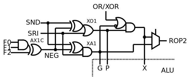
From there, you "just need" a pair of MUX2 and you have ROP2 again. Which is pretty alluring. However MUX2 is not a trivial gate in ASIC so there must be a better way to do that, right ? :-)
Indeed (bis) you can do it with an OR gate to force-enable the G signal before it gets ANDed into the X signal. There, you have now 2 output signals that provide AND, OR and XOR. A MUX2 gets this down to 1 signal.
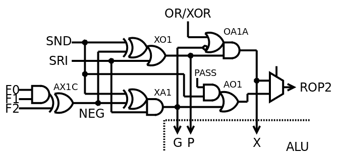
There is a "free time slot" between the XA1 and MUX2 which can be used to implement the last function : SET/pass. Since it's the output of a AND, it's easy to apply the same idea as before: one of the operands (SRI) can be restored by ORing it back, selectively (though a AND).
But then, things get, hmmm...
The circuit is great but the control signals require a non-trivial amount of changes.
One consequence is that I have to change the order of the ROP2 opcodes.
The SET/pass feature is in the datapath of AND/ANDN so one of them must be "mirored" with SET. I chose AND as 0000 because ANDN is better left as 0011, to keep NEG's decoding logic simple. This creates the weird situation where OR and XOR are stuck between AND and ANDN, which is solved by decoding F0 xor F1.
| Opcode | F3 | F2 | F1 | F0 | Pass | NEG | OR/XOR | ROP2 mux |
| AND | 0 | 0 | 0 | 0 | 0 | 0 | × | 0 |
| OR | 0 | 0 | 0 | 1 | × | 0 | 1 | 1 |
| XOR | 0 | 0 | 1 | 0 | × | 0 | 0 | 1 |
| ANDN | 0 | 0 | 1 | 1 | 0 |
1 | × | 0 |
| CMPU | 0 |
1 |
0 | 0 | × | 1 | 0 | × |
| CMPS | 0 | 1 |
0 | 1 | × | 1 | 0 | × |
| SUB | 0 | 1 | 1 | 0 |
× | 1 | 0 | × |
| ADD | 0 | 1 | 1 | 1 | × | 0 | 0 | × |
| SET | 1 | 0 | 0 | 0 | 1 | 0 | × | 0 |
The final equations (some already known) are easy to deduce:
PASS  = F3
NEG = (F0.F1)xor F2
OR/XOR = /(F1 | F2 | F3)
ROP2mux = F0 xor F1
ROP2/ALUmux = F2
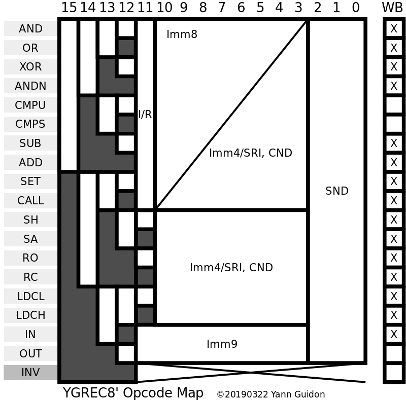
And we get the following updated table :
Time to change some VHDL definitions now...
The assembler is not much affected (autotests passed) because in practice, only AND and OR have been swapped. The ALU code however needs much more work...
For historic references, look at that analysis of a WANG computer.
_
Discussions
Become a Hackaday.io Member
Create an account to leave a comment. Already have an account? Log In.