 Yann Guidon / YGDES
When you create you processor, you want it to work, then priorities shift to speed because the processor must be compared on its merits. Then... it's over, it's too late, the infernal bikeshedding machine is in motion and hard to steer.
One thing is sure, however : the industry has spent the last 15 years steering toward energy-efficiency, toward more MIPS per Watt and it's often overlooked in the early drafts for amateur designs. We don't care how much our pet machine will consume, since it won't run that long or that much. But efficiency is a staggering goal, even more than performance because today we have so much power at our fingertips. But think about this : if your processor runs 2× slower but uses 3× less energy, you are actually winning and you can put 2 or 3 processors in parallel easily.
Energy efficiency is not a significant goal for the #YGREC8, nor is performance, or else I wouldn't bother with a relay version. I don't expect the ASIC or FPGA version to run on a battery but you never know. It's never too early to build this into a design that is intended to be the basis for larger designs... And those designs will want to avoid using a heatsink.
Today, CMOS is the dominant technology and the initial target of my designs, either in FPGA or ASIC (the rest is for the lulz). Its consumption is proportional to three main parameters C-T-V :
- power supply Voltage (squared) : reducing the voltage is a simple and easy way to reduce the power, to a certain extent at least, because the out-of-range values will not allow the circuit to run fast (or at all).
- Capacitance : the gates of the transistors act like capacitors that must be charged and discharged. The capacitance drops as technologies shrink, which we can't control easily, but as a rule of thumb: the more transistors are toggled, the more they will consume. That's an interesting angle of attack...
- Toggles : the faster you run the circuit, the more charges and discharges, the more energy is needed to switch the transistors. Energy-saving methods often include running the circuits slower.
Some of those parameters are in the realm of the implementer. For example, the supply voltage or the frequency will not directly affect the logic of the circuit (within the nominal operating conditions of course).
Some other parameters are directly under the control of the designer, and can be summarised as : toggle less, less often.
I have mentioned running the circuits slower, but there are other methods as well, some belong to the purely digital design real, others on silicon sorcery, such as playing with a voltage bias with the bulk of the substrate, altering the temperature, changing the doping or composition... Let's forget them.
What matters at this level is what we can do at the architectural level. We can't control the clock speed in the absolute, but any design choice affects either latency/speed or consumption, usually both. And this is relative.
One textbook example is "clock gating" : drive the clock input of the group of DFF that really need to be updated. It's easy to do, and easy to mess up, because it's at the edge of timing analysis and FPGA prefer "clock enable" with one main clock.
Clock gating is finely tuned in very low-power devices. Years ago, I heard of a complex processor being split into more than a hundred of clock domains and I'm sure the numbers are much higher today with Intel's latest processors, where not only clocks, but power domains are fine grained. But this technique is not easily portable.
The YGREC8 has other places where some "toggle optimisation" can be effective and easier to design, given the proper framework and structures. One such example appears in the ALU where several control signals not only have to be propagated to 8 (or more) logic gates (a fanout of 8 is not negligible) but the results of the changes will propagate through the rest of the datapath and logic gates. Some bits might not change, some could toggle back and forth during the cascade through the adder... Any change at the input or the control signals of the adder can create an avalanche of short spikes that will consume power.
The truth table of the ALU control signals (processed in the decoding unit) has many "don't care" states, which are currently used to save latency through logic minimisation. These "don't care" states could instead behave as "don't change" in an alternative version of the decoding unit. It's just a matter to keep the propagation time short and the logic simple.
As previously discussed, using DFF or transparent latches would not work, because of timing analysis and increased latency. Fortunately, these are not the only types of FlipFlops and the solution might be even simpler than that :
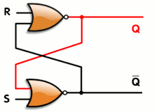
The SR latch has one gate of propagation time and the synthesiser will only complain about looping back the output (you can nicely tell it to ignore the situation with some pragmas).
The S and R inputs will be driven by different/separate combinatorial circuits that will only change the output when really required. The remaining input combinations will leave the output unchanged. This can be written in VHDL with code like this:
signal <= '1' when (condition1 OR contition2)    -- SET
     else '0' when (condition3 OR condition4);   -- RESET
     -- no final "else" value !
The synthesizer will not be very happy and will try to generate weird stuff. It needs "some help" to swallow the pill and good coding practice will lay out each equation for SET and RESET, then input them in a custom SR latch, using a lower level description.
In the case of the A3P family (and probably others), there is an extra bonus that uses only one gate/tile instead of 2 NORs :

This is the OA1B gate looped back to itself. The SET action will be a little bit faster than when using 2 separate gates.
The decoding logic will certainly have more depth than the "optimised for speed" decoder but the decrease in electric activity is worth the slight delay. The fun part is that the SR latch method is retro-compatible with the optimised version and there is no added constraint (no need for more inputs for example). The two versions are easily interchangeable and could even be switched from one to another on the fly for a "turbo" mode...
For a useful example, let's have a look at the boolean map of the ALU in the log ROP2 reloaded:
| Opcode | F | Pass | NEG | OR/XOR | ROP2 mux |
| AND | 0000 | 0 | 0 | × | 0 |
| OR | 0001 | × | 0 | 1 | 1 |
| XOR | 0010 | × | 0 | 0 | 1 |
| ANDN | 0011 | 0 |
1 | × | 0 |
| CMPU | 0100 |
× | 1 | 0 | × |
| CMPS | 0101 | × | 1 | 0 | × |
| SUB | 0110 |
× | 1 | 0 | × |
| ADD | 0111 | × | 0 | 0 | × |
| SET | 1000 | 1 | × |
× | 0 |
The speed-optimised equation for PASS is F3. The toggle-optimised version is
PASS_SET <= F3 and not F2 and not F1 and not F0;
PASS_RESET <= not F3 and not F2 and not (F1 xor F0);
It's quite more verbose and longer but not exceptionally so. More such boolean calculation can be factored with a sort of PAL-like array.
OR/XOR, like the others, takes each result value apart and groups them in the SET and RESET equations:
ORXOR_SET   <= '1' when  OPCPDE=Op_OR else '0';
ORXOR_RESET <= '1' when (OPCPDE=Op_XOR
                      or OPCPDE=Op_CMPU
                      or OPCPDE=Op_CMPS
                      or OPCPDE=SUB
                      or OPCPDE=ADD )
                        else '0';
it's not really complicated when an explicit declaration is used.
ROP2mx can also be rewritten with split SET and RESET equations:
ROPmx_SET <= '1' when (OPCPDE=Op_XOR
                    or OPCPDE=Op_OR )
        else '0';
ROPmx_RESET <=  '1' when (OPCPDE=Op_AND
                       or OPCPDE=Op_ANDN
                       or OPCPDE=Op_SET )
           else '0';
Do you see now how it works ?
Update:
To better work, the decoder needs an "instruction enable" latch signal that arrives late enough to prevent glitches inside the decoder itself, but not too late either. It must also be controlled by the FSM because not all outputs from the Instruction Memory are instructions (think LDCx...)
Discussions
Become a Hackaday.io Member
Create an account to leave a comment. Already have an account? Log In.