Update 20200714 : see the follow-up 107. Choosing the gates
See also http://www.vlsitechnology.org/html/le_intro.html.
Reader warning : this log/post touches the fundamental things that make me the most passionate about digital design and architecture. Playing with TTL chips, relays and transistors is a fun game but here you have a glimpse of some damned serious matters. This log justifies several aspects of my design choices so strap you belt and learn a few things.
I aim at building the YGREC8 with various technologies (mainly for fun and giggles) but with the same ISA, so the different implementations can execute the same programs, as well as with the same structure and even the same gatelist (except for the relays version). This means that I focus on the manual synthesis of the design and I break down every function down into individual gates. I choose the lowest common denominator for the chosen technologies and then I reuse the same gatelist without trying to overoptimise too much for each target...
This means I must also choose the right structures and keep them (except for the relays). For example, the ALU will be (mostly) identical, with the same CLA because I don't want to re-engineer the system for every new implementation.
The ProASIC3 and the relay versions favour the MUX2 as the atomic, do-everything gate but I intend to use ASIC/CMOS as well as bipolar discrete transistors, which require simpler gates.
- Bipolar gates really prefer the NAND function. It's really the simplest, so it should be the fastest...
- CMOS ASIC technology loves both NAND and NOR (they are symmetrical) but they have a practical limit for the number of inputs. Apparently 3 is a compromise between size and speed because more inputs would put too many pass transistors in series, which would slow down the gate, or force the channel to be too large to compensate (and increase capacitance).
So the "preferred gates" are NAND2 and NAND3.
Others like latches, NOR, INV and XOR are accepted where needed. For example I have studied the structure of the latches and XOR in several previous logs on other projects (for example the XOR zoo)
Having more inputs to the NAND would be a big benefit to reduce the size and increase the overall speed:
- This lets MUX have more inputs and fewer levels, which is better
- The carry lookahead (and incrementer) can have a coarser granularity, fewer levels and a shorter critical datapath
- and I probably forget a few other units, SHL would be a good candidate as well.
Bipolar discrete circuits can have many inputs, 4 would not be a concern, maybe 8 is possible before running into signal integrity issues. The question is: is it a good choice for CMOS ?
I have recently received an answer from @Staf Verhaegen :
"Multi-input cells are mainly power and area optimization and not performance. Area optimization is trivial due to reduced number of transistors; power optimization is due to the removal of internal switching nodes.
I haven't looked deeply in maximum number of series transistors in a design but typically one does not go above four. Going more would need big transistors and likely not that much would be used by synthesis anyway."
Thank you for the context expansion :-)
Let's see how/why this is so.
CMOS obeys to a few rules, in particular t=RC so the goal is always to minimise resistance and capacitance.
Capacitance comes from the gates regions because the thin area where the poly overlaps diffusion creates a capacitor. The smaller the gate, the faster.
However resistance comes from the relative width of the area through which current flows. The smaller the section, the less current flows, so the width must be maximised to make fast circuits.
So there is this basic compromise : if you make a transistor wider you increase the current hence the speed but this also increases the capacitance, which reduces the speed...
And this is for one transistor. CMOS gates need transistors in parallel and series ! And the more inputs, the more in series, and the more resistance, which also reduces the speed...
- 2-input gates are a bare theoretical minimum for making a circuit. You won't go far with 1-input gates.
- 3-inputs gates are an extension of the 2-inputs version. Just enlarge the gates a bit to keep speed in check.
- 4-input gates can concentrate more values but need 2× larger gates than the 2-inputs version to keep the speed. But 2× larger gates also means 2× RC delay, 2× the drive strength and/or 2× the propagation time. A compromise is required such as 1.5× width for about 1.5× increase of delay but this also requires spraying the chip with more buffers/inverters to boost the signals anyway.
conclusion 4-input first-kind gates (NAND4 and NOR4) are good for reducing the power and area (hence costs) but don't help with performance in CMOS. That would however be an interesting option for a power&cost-enhanced version, where NAND4 is preferred every time it's possible. And given today's technology, that power reduction could have great benefits, as AMD found with their latest CPU generations : reducing the power allows you to pack more cores than the loss of individual performance.
Of course it's still possible to plug some 4-input gates at some critical places to "get things done". For example the current SUXEN has a MUX3 and doesn't get the SHL unit. Adding a NAND4 would add the SHL easily into the result bus. Upon closer inspection, PC+1 need to be sent as well so another layer of MUX3 would still work well...
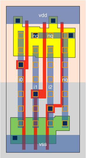
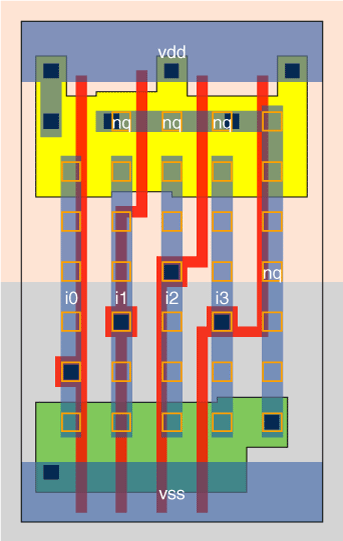
I find AND4 and NAND4 in some standard cell libraries. For example, the SXLIB has NAND3 and NAND4 gates :


The size bloats however when a higher output driver strength is required, with 2 inverters...
However, increasing the number of inputs also increases the density of the control wires and it can increase the difficulty of routing. It's all a matter of balance...
Looking at the above cells I notice that there is quite a significant area that is not used by the diffusion. This could save 20 or 30% of total die area if it was trimmed, with corresponding savings in costs and probably speed. This area is used by more complex gates that need more internal logic layers (XOR, DFF...). So I wonder if/how it is possible to make a "reduced count" gate library with only "low-profile" gates... A sort of "RISC" method applied to CMOS ? :-D
 Yann Guidon / YGDES
Discussions
Become a Hackaday.io Member
Create an account to leave a comment. Already have an account? Log In.