 Yann Guidon / YGDES
Today, after I designed the large MUX, I validated the part of the TAP that extracts information out of the core.
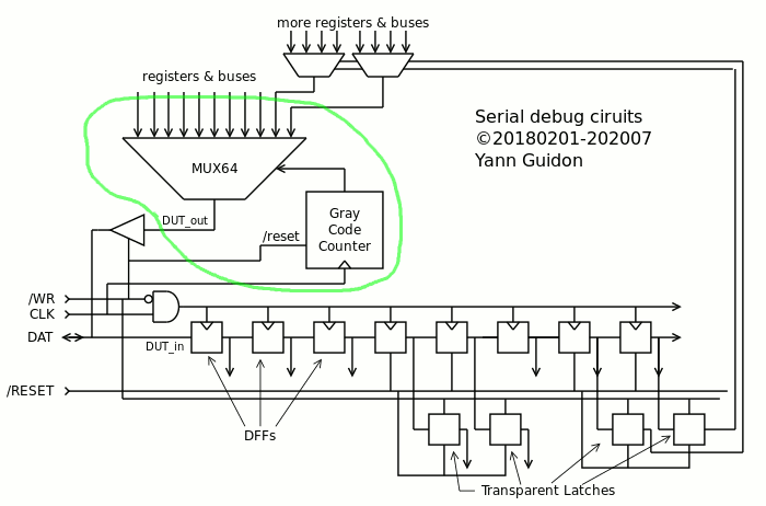
The Gray+BBT-BC combination has very good characteristics (fully asynchronous, glitch-free, easy to route, no select/clock/reset fanout problem) but at the price of some serious scrambling so I wrote the tools to extract the scrambling/permutation vector. Now the program test_readback.vhdl shows that I can reconstruct the original value from the serial output bitstream.
The vector is stored in the file PISO_permutation.out as a series of comma-separated decimal numbers and can be #included in other source code files. This file must of course be updated if the structure of the tree and the type of MUX are altered.
In practice, there are two uses :
- shift bits in, 64 at a time, to get a snapshot of the selected signals. The 8 bytes must be descrambled together to make any sense.
- Select one signal and spy on it with a 'scope for example. It could help with asynchronous signals, IRQ, event counters...
The extra optional MUXes are managed by other parts of the circuit, which are target-specific
The other half of the TAP is similarly split into a common/generic/core part and a target-specific one that can be adapted later. It is not shown on the above diagram yet but we can already see 2 cases :
- some values of the shift register are transient and it's OK. Usually, these values are then MUXed with other internal signals and sampled when the core is stopped for example. So there is only the need of one DFF in the chain (you handle the MUX where you want).
- some values must be persistent : their alteration during shift would just "confuse" everything so an additional memory cell is required. For example they hold a control code, or drive MUXes. The extra cell is is not necessarily an edge-triggered DFF because the value is already stable and the latch is controlled by /WR, not CLK : there is plenty of setup&hold margin there. A transparent latch is smaller and sufficient.
So two types of scan cells are required (persistent and transient), one with an extra latch. They are instanciated by the higher-levels of the system.
At the lower level however we can already provide safety features that also ease the rest of the design. The first thing to ensure is that the received bitstream is valid. A CRC would require too much effort (particularly on the control/host side) but a small signature is almost as effective (it doesn't provide signal integrity but the format is easily checked). And there could be several signatures, right ?
The "signature" so far is a byte that is shifted in at the end of the bitstream, as a suffix : the 8 bits are always held by the core TAP circuit and the value is examined last, before /WR goes up. A simple boolean circuit can then check if the latches may be updated.
And if there are several signatures, different sub-groups of latches can be selected ! New groups of latches are then formed from unused signatures to provide upwards compatibility. Invalid signatures are ignored and don't update the internal state or latches, yet affect the shift register.
The signature/select byte can take an easily-recognised value, which we can look up in the ASCII table.
- The letter T comes first to mind, for Test : 01010100 is a nice-looking binary word, right ?
- Do you want to read the Events ? type E, or 01000101 to write to the related latches.
- Are registers interesting ? Try R : 01010010
- Bus : B = 01000010
- Core : C = 010000101
- Inputs : I = 01001001
- Load instructions : L = 01001100 (to feed into the instruction SRAM before the CPU boots)
- Outputs : O = 01001111
- etc. (you get the idea, and there is a significant addressing space)
The beauty is that this is a suffix value, sent just at the end of the data stream, before /WR goes high again. This control word will then select auxiliary MUXes for example. The control word as well as the end of the shift register can be read back from the PISO to provide a loopback feature and a simple sanity check for the debug system.
And as usual this releases pressure from the clock and RESET tree, as only a few essential signals require the /RESET line and the clock is inherently split into separate low-speed groups that are easier to place & route.
Simulation on Falstad validates the ideas :
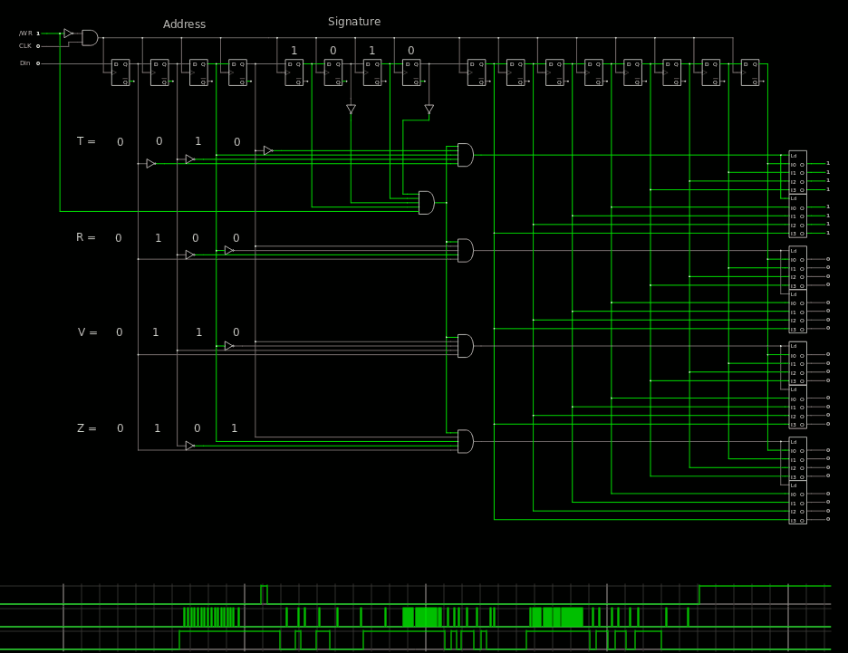
In the above example, I have set all the "T" output by sending 0xFF followed by the 'T' character (MSB first). Setting /WR to 1 activates the latch/buffer while the others are left in their previous state.
This works despite the fact that the quad "latch" component of Falstad is edge-triggered : the group Enable signal is valid only when /WR is high, but it must go low before new data may be shifted in (and this is when the data is really latched and kept). At 10MHz there is enough setup&hold margin to prevent timing issues.
If you are unsure why all these efforts, compare the size of a MUX2 ASIC cell (which can be looped back to itself to make a T-lach) :

With the size of a classic DFF cell :

Some of these also require a RESET signal so the system is powered up in a coherent configuration, but that's a detail for another day (the YGREC8 only needs its internal FSM to be cleared and the rest follows, no need to spread a RESET signal all over the register set for example).
Overall, compared to JTAG, this type of TAP maps easily with short requests from debuggers for example. More complex features are then built as combinations, "sentences" of short messages. There is no internal FSM, no need to scan the whole chain just to get one value... OTOH it is not designed to be easily chained.
But this is not the end of the story, far from it : look at Design of a TAP : the SIPO Controller.
Discussions
Become a Hackaday.io Member
Create an account to leave a comment. Already have an account? Log In.