 Yann Guidon / YGDES
As I am near completion the design of the TAP system, I realise I have harder and harder timing problems to solve... And I could even save some gates !
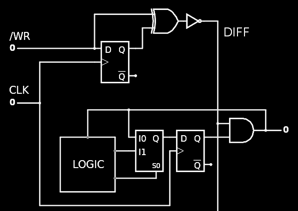
The Counter has 32 gates. The Gray counter has 17. Both count on CLK's rising edge and mayyyybe... they could be merged ?
It's not difficult to adapt the Gray counter to provide the additional signals FB (Full Byte : just a NOR3) and SAT (an added DFF and a couple of gates), as well as individual decoded size output signals for 1 to 8 bytes (though so far only 2 and 4 are used). Overall, the Gray counter would expand to maybe 30 gates, which would overall save maybe 20 gates compared to the split design, and the DFF would not have a RESET input, which might be absent in ASIC gates libraries (and use more silicon)...
The harder part though is the transition between the 2 phases and the reset of the counters. I think I have an idea but it will force me to deconstruct the Gray counter into a more traditional logic+DFF system, because... it will become a classic digital sequential circuit, with the current state and the expected new value that may (or may not) be latched.
20200808 :
Some more thoughts gave this result :
This easily solves the question of using the counter with BOTH phases, at the cost of 1×DFF, 1×XNOR and 1×AND2 per counter DFF.
Here is how it shoul look with wavedrom :
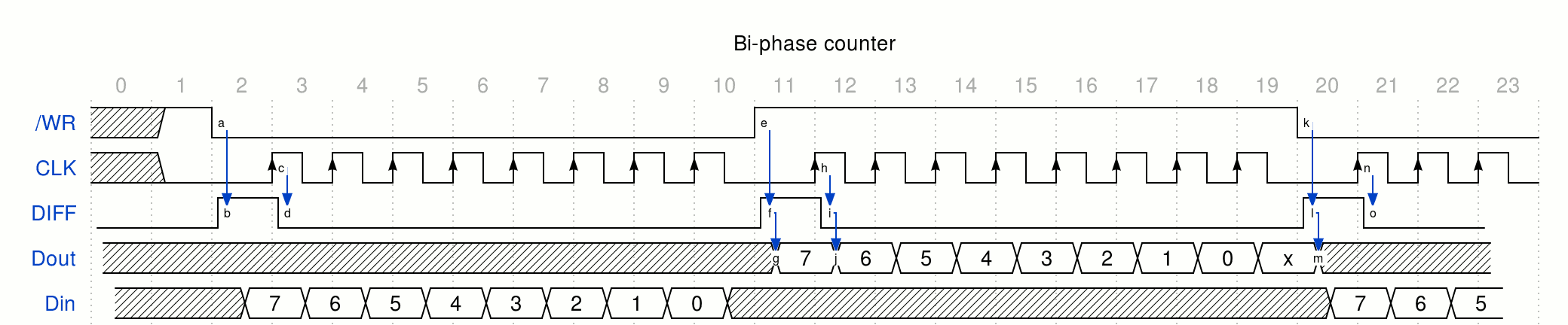
This does not solve however the case where /WR is toggled up and down without CLK activity. The DIFF internal signal should be "sticky" and go back down when CLK has a rising edge...
There, it should work now :-) (ok it doesn't because of a race condition with the clock)
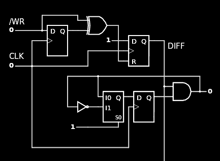
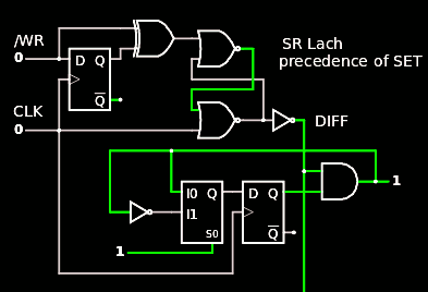
Each time /WR changes, the added DFF is RESET, and later set again by a positive edge on CLK. The question now is how to emulate this DFF with individual gates. The following circuit seems to work well and is adapted to ASIC implementation :
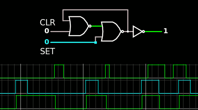
The two NOR2 use little surface on a die. The output inverter works as a buffer. There is no oscillation condition, as proved in the above trace : the SET has precedence over CLR, which avoids the race condition found with the initial idea using a DFF. The initial value of the latch is determined by toggling the /WR and CLK pins and a short initialisation sequence brings the circuit to a know state:
- bring /WR low
- pulse CLK once (at least, could be more) => first DFF state is known
- set /WR high => changes XOR => CLR the SR latch
- pulse CLK once (at least, could be more) => SET the SR latch
The output data can be ignored, shift 0s in to make NOPs (just in case). So this could be summed up as : shift a NUL byte in, then shift a dummy byte out.
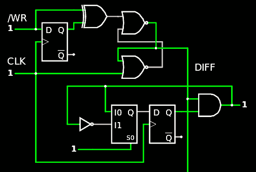
Here is the new version :
Note : this works ideally when the CLK input is LOW when /WR changes. However : to create a rising edge, CLK must go down before going up again, this half-clock phase (when low) will be the "clear state". Ensure this period is long enough and that the CLK state is appropriate (check on the 'scope to be sure !!! I'm looking at you, Raspberry Pi...). This is not critical while shifting bits in, however it is a delicate thing to ensure when reading from the TAP (in particular, the first "volatile bit").
This is solved by changing the precedence of the RS latch to RESET/DIFF/WR, as in this updated circuit :
And the extended chronogram :
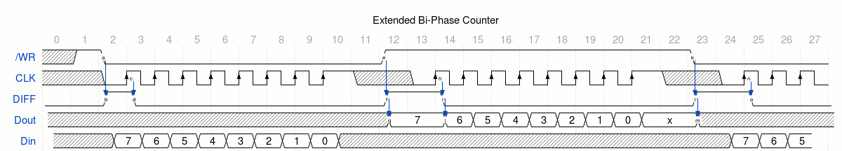
Now CLK can go low before or after /WR changes.
Just by changing where a wire is connected.
Discussions
Become a Hackaday.io Member
Create an account to leave a comment. Already have an account? Log In.