 Yann Guidon / YGDES
It seems that the "main schematic" below, used as the project's avatar image, is not obvious enough, at least before zooming in enough.
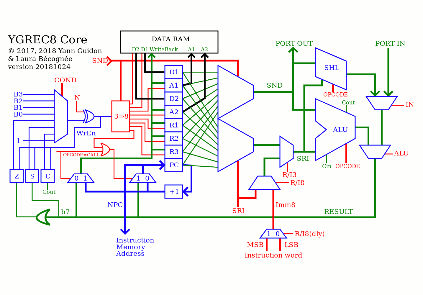
@Ken KD5ZXG was not sure how to interpret/decypher the upper-left side.
- I see YGCREC8 mux between Carry Sign Zero Always and the lower four bits of B. What is B? I get what Write Enable and N are for, but how do these interact with the tested condition to drive some rectangle called 3=>8 that I might guess 8 way mux if you hadn't already drawn other mux with the proper symbol. Maybe the 3=>8 rectangle is just a decoder? I've got a condition mixed with N thats probably one of the 3 selects, a write enable thats not clear how it works (chip enable?), SND whose purpose remains a mystery drives some other select bits? Enlighten me, cause I'm clearly not getting it.
So here is the explanation.
- The 4 basic conditions are ACSZ, as already obvious. I now use the alphabetical order for convenience and mnemotechnic help.
- The 4 extended conditions are optional and user-configurable: either fixed (if you have 4 input/GPIO pins or other internal signals) OR you can implement a set of Special Registers that select the source of each condition bit. This is one of the tricks inherited from the YASEP.
The home page says :
- Always
- Z (Zero, all bits cleared)
- C (Carry)
- S (Sign, MSB)
- B0, B1, B2, B3 (for register-register form only, we can select 4 bits to test from user-defined sources)
The COND field has 3 bits (for Imm4) or 4 bits, more than YGREC16, so we can add more direct binary input signals. All conditions can be negated so we have :
So this extra condition bit allows extensions for later, which could speed up some IO intensive algos, such as bit banging. "B" means "bit", it's not a register per se (though it must be latched before to prevent race conditions) and it is user-defined wires. They could be front panel switches, synchronous or asynchronous data over 1 or 2 bits... or some condition inside the extensions blocks like UART ready/overflow/whatever status bits. I was a bit inspired by the CDP1802 on this, I admit.
The "Never" condition could be mapped to another bit/wire/condition but I don't want to play this game yet. ARM mapped this to an extension to the instruction set but YGREC8 is too young for that gymnastics yet.
... Maybe the 3=>8 rectangle is just a decoder?
Yes, once the condition for writing the destination register is determined, it is sent to the appropriate destination register for writeback. I should have made it clearer but the drawing is already pretty crowded :-)
The register set uses latches, and not DFF, to cut the register set power/area/cost in half. Imagine routing the clock signal to 64 bits and only updating 8 (or 16) every time... The diagram misses a buffer latch on the result datapath btw.
I'll try to summarize :
- First the condition must be evaluated. It is by default 1 : enable. The XOR can negate the condition when needed, directed by the relevant bit in the instruction word (in red). The condition can be any of A/C/S/Z/b0/b1/b2/b3 (the B conditions are optional as noted above). So it is quite simple : we have a bit that is usually 1, but also selectively cleared.
- The condition is valid at the output of the XOR. Then this signal will
- enable the update of the C/S/Z condition flags
- go to the 3=>8 decoder to enable and select one byte of latches, so the relevant register (indicated by the SND field) is written (or not).
.
I hope it helps.
Discussions
Become a Hackaday.io Member
Create an account to leave a comment. Already have an account? Log In.