 Sundance Multiprocessor
One first fundamental step was to develop a custom IP core in order to interface with a CameraLink camera. In our demo we used a Sentech STC-CLC83A camera, which has a resolution of 1024x768, 30 fps, 8 bits per pixel, Bayer color scheme, BASE only configuration.
For the video output section, we used an existing simple IP for HDMI output, which we just modified slightly to adapt to our case. HDMI output signals interface with the ADV7511 chip, which needs to be configured by software on startup. HDMI is available through Sundance External Interface Connector add-on board. The output settings fit XGA standard: 1024x768, 60 fps, RGB.
Hardware Design
In this section we'll summarize the steps taken in developing the hardware firmware. Our project is based on Xilinx's SDx 2017.1 design suite.
FC500 CameraLink IP core
As first step we needed to develop an IP core in order to interface with our CameraLink camera. This is the overall scheme of such IP:
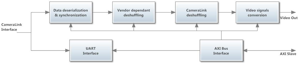
Data serialization is a fundamental step in order to get the 28 bit word from four serial data lines with serial factor 7x. Video signal conversion generate active video, hsync and vsync in a format compatible with other standard Xilinx IP core.
UART interace is fundamental in order to communicate with the camera and initializate it from software.
Here is the IP core web page:
http://www.sundance.com/product-range/sundance-products/ip-cores/fc500-cameralink-ip-core-for-zynq/
Overall architecture
The following figure shows a simplified view of our hardware design, developed using Vivado 2017.1:
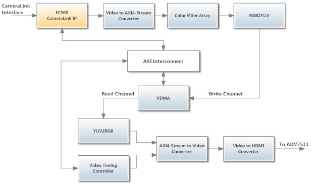
The orange coloured IP is the FC500 IP core discussed previously. Our design also includes the Zynq Hard Processing system, not shown here for space reasons.
The FC500 IP core output video data (8 bit per pixel), Active Video, Horizontal Sync and Vertical Sync signals. The Video-to-AXI4-Stream-Converter converts such signals to AXI Streaming Bus signals, which are compatible with several AXI based video processing IPs. We used then a Color Filter Array IP to convert the Bayer color mosaic into a standard RGB signal (24 bits per pixel). This RGB signal is itself converted to YUV 4:2:2 format (16 bits per pixel) in order to facilitate processing based mainly on luminance component. In such format frames are stored in DDR memory by the VDMA. For this demo we used a triple buffering mode.
In the output section (lower part of the figure) we find some 'inverse' operations with respect to the input, plus a Video Timing Controller, which generates the correct sync signals for the chosen output format (XGA 1024x768, 60 fps), and an HDMI output IP, which makes just some signal adjustments and DDR modulation for the ADV7511.
There are three main clock domains:
- CameraLink clock: this is an external and therefore asynchronous clock which needs to be synchronized using IDELAY and ISERDES components plus an FSM. For our camera, its frequency is 30 MHz.
- HDMI output clock: its frequency matches the one required for XGA pixel clock (explained previously) and it's 65 MHz.
- AXI Bus clock: we chose its frequency to be 130 MHz, which is more than 100 MHz (cosidered as minimum requirement) and its the exact double of HDMI clock frequency. This setting helped meet clock domain crossing timing constraints.
Other secondary clocks are for example a 50 MHz used for the CameraLink UART interface and a shifted version of the HDMI clock, which is the one actually fowarded externally to the ADV7511.
Software Design
Using Xilinx SDK 2017.1 (subset of SDSoC) we created a Board Support Package for our hardware project. This can be used to generate bare-metal application projects.
Then we created a Hardware/Software platform to be used for SDSoC high level synthesis projects. We used the SDSoC Platform Utility to generate a platform for bare-metal (standalone) oriented application projects. A custom platform TCL script must be supplied, beside the hardware project and BSP files.
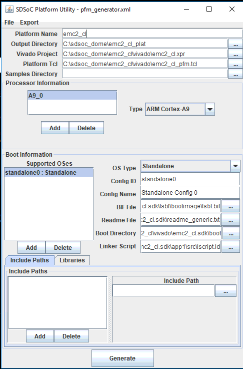
When a new platfrom is correctly generated it can be imported in SDSoC and used as base for new Application projects.
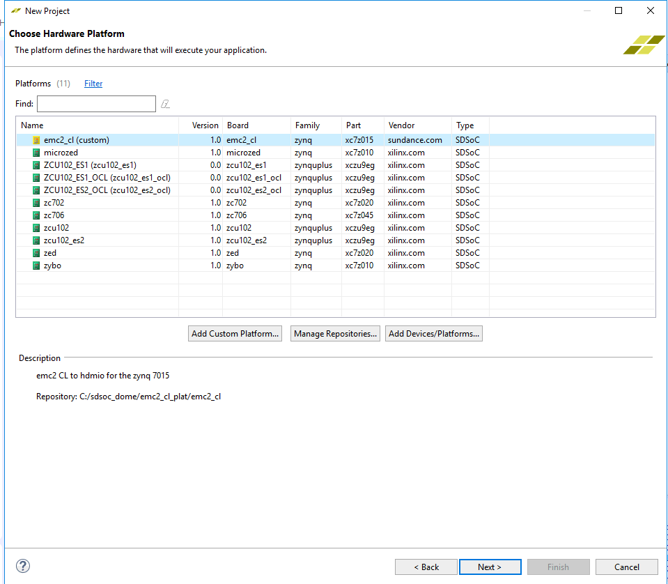
More precisely, it is possible to choose a predefined platform or specify a custom one:
Our application software presents this overall structure:
- Initializations
- Menu
- Sobel filter
Peripheral initializations involve these components:
- ADV7511 (through HPS I2C interface)
- FC500 CameraLink IP
- Video Timing Controller
- Interrupt
- VDMA
A menu is printed at the serial terminal, containing the following choices:
- Passthrough mode
- Full-screen Sobel filter
- Half-screen Sobel filter
Sobel filter code shows an example of the advantages of hardware acceleration. Its code is written in simple C language but it is selected in SDSoC project options for hardware acceleration. While building the project, this function is processed by High Level Synthesis tools to be mapped to hardware. This yield far better performance than software only implementation.
When the filter is accelerated, the main purpouse of the software code is to control the advancement of VDMA frame pointers. More precisely, the VDMA is used is parking mode, that is, we set the frame on which each channel must stop(or "park") and not going further. We using triple buffering and set the frame pointers so that the read channel, the write channel and the Sobel filter all work on different frames, so removing every glitch or artifact, such as stuttering. Once the Sobel filter (both in software of hardware accelerated) computing is finished, all VDMA frame pointers are manually increased by software code, so to show the new computed frame and compute the Sobel filter on a new input frame.