 Craig Watson
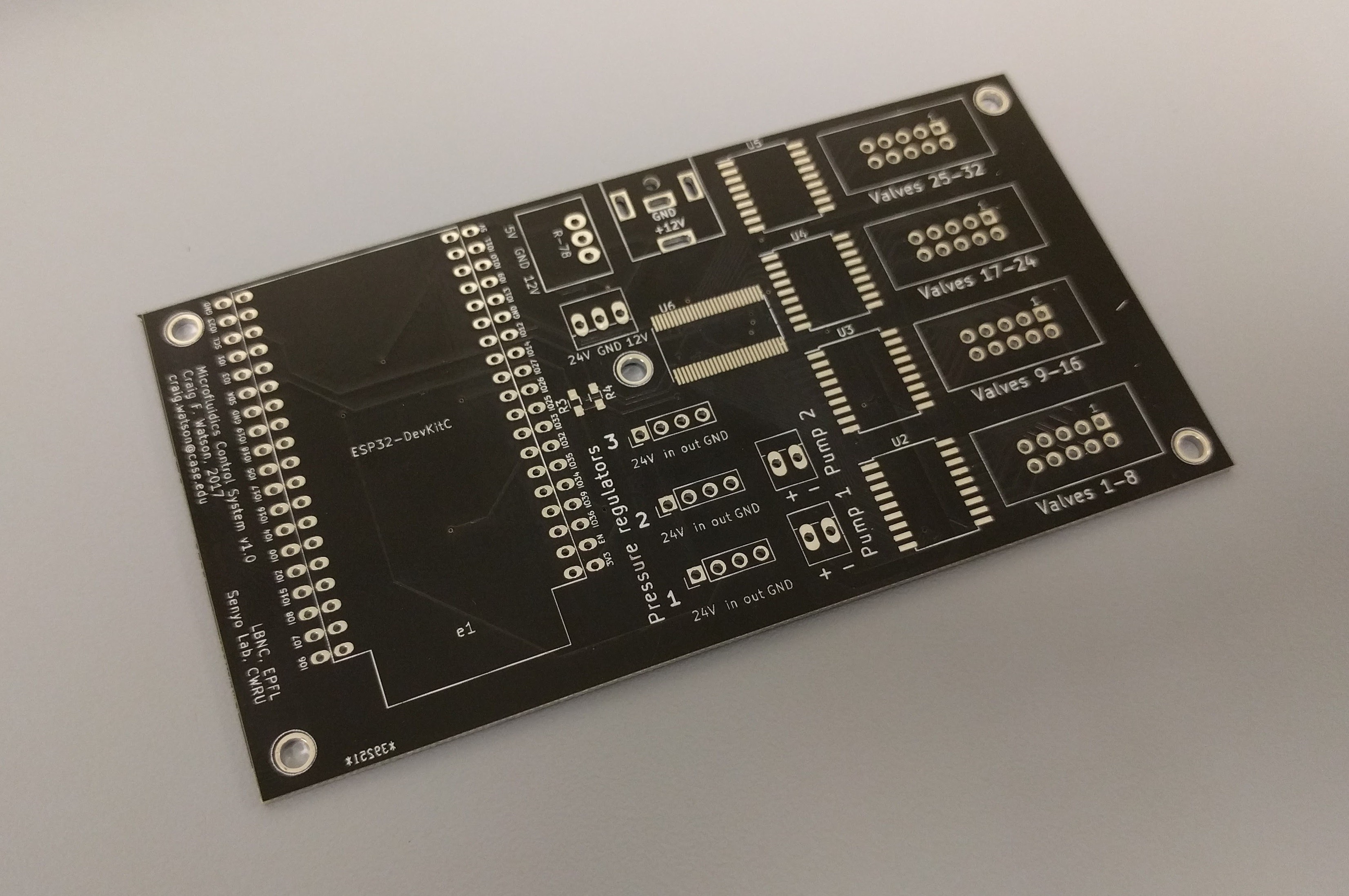
With the PCB design finished, double-checked and triple-checked, I ordered some boards on DirtyPCBs.
This is a ridiculously cheap service; it was even cheaper than OSHPark and any other manufacturer I found. I got around 10 boards for 29$ + 6$ shipping.
One concern I had with the manufacturing was the minimum soldermask size. The PCA9698 (IO expander) has a TSSOP-56 package, which has 28 pins on each side, with a pitch of 0.5mm. That leaves very little space for error, and having soldermask between the pins helps to avoid bridging when soldering.
I thought my PCBs would have this soldermask, but either I was mistaken when reading through DirtyPCBs's specs, or I made an error in my designs, because they arrived with no soldermask between these pins.
Luckily it turned out to be easier to solder than I expected, and a little wick was enough to fix the few errors I made. This step, by the way, would not have been possible without a microscope to help with soldering and inspecting. Thankfully, our university has an amazingly well-equipped makerspace that has some good irons and a couple of microscopes.
Soldering the rest of the components was rather straightforward, and so after a couple of hours, I was able to turn this:
Into this:
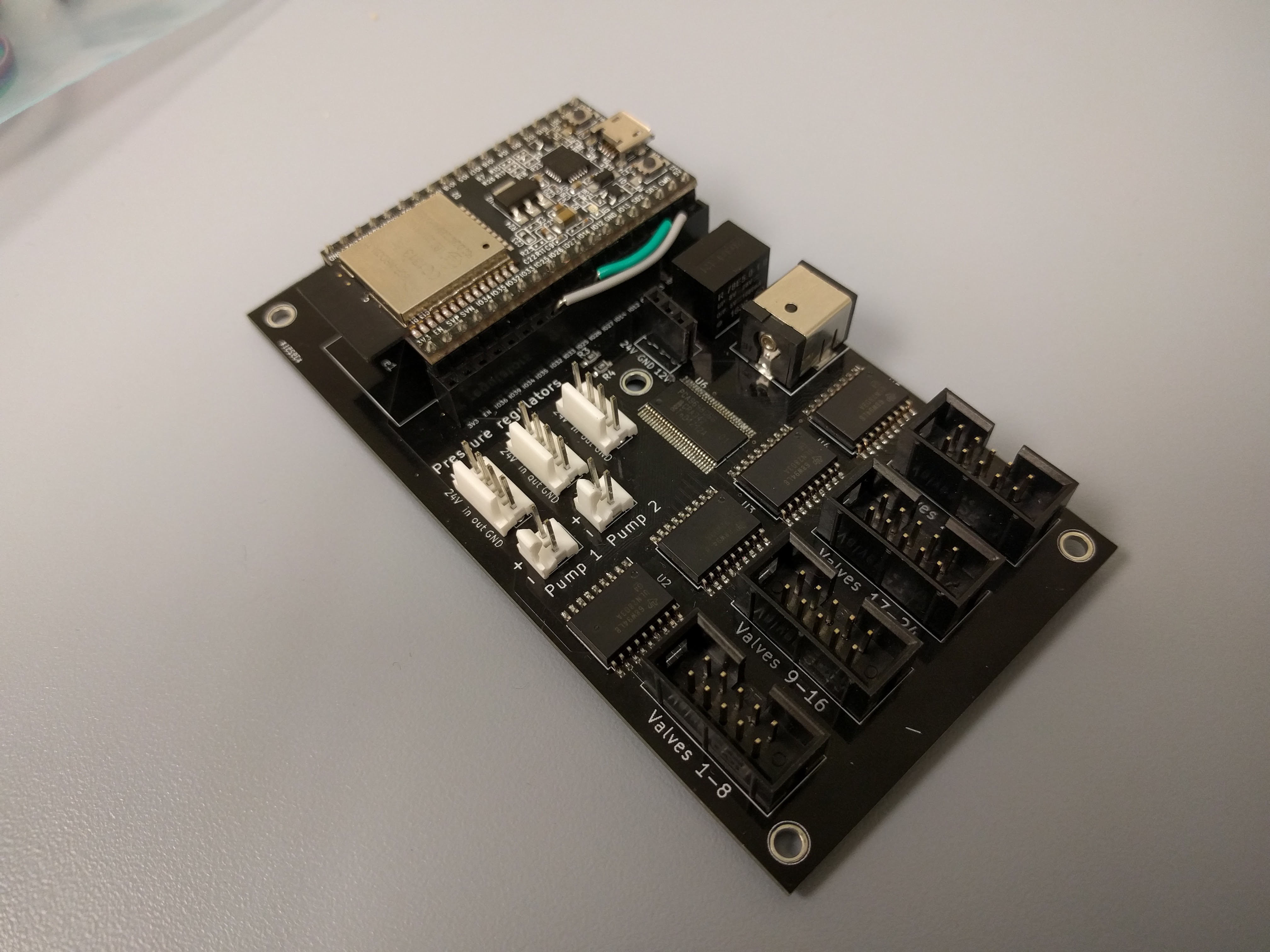
The ESP32 is sitting in some female headers I put in so I could easily make modifications or plug other things in. As you may be able to tell from the jumper wires, that came in quite handy.
Just after soldering the last components, I noticed this:
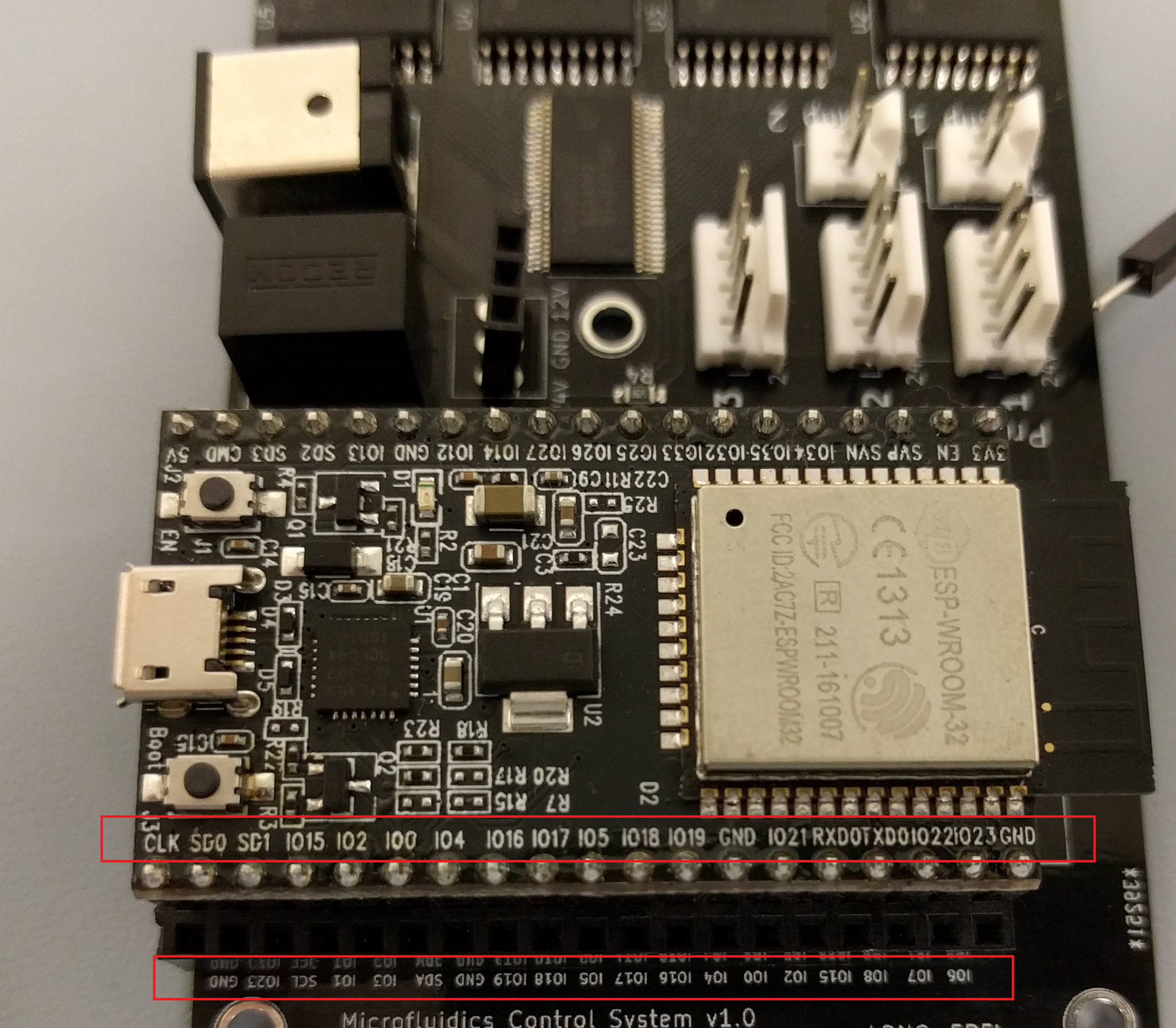
PSA: check the orientation of your datasheet when you design a footprint.
Luckily for me, that side is only used for a few pins: the SDA and SCL lines for I2C, and a couple of ground pins. So the fix was a relatively simple matter of desoldering the headers, cutting them and putting just a few back, for the actual SDA & SCL lines, and using some jumper to connect the old pins to the new, correct ones.
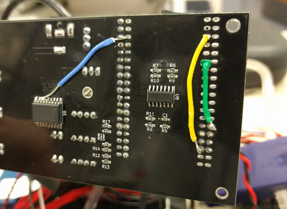
The yellow and green wires correct my poor design skills; the blue wire, to the left, was added after I accidentally nicked a trace while repairing some other issues.
The other hardware issues were:
1) The pins labeled as GPIO9 and 10 on the ESP32 datasheet cannot actually be used as GPIO. They serve only for Flash. This is why you can see jumpers in the second image, above.
2) I connected the ESP32 dev board's 5V to the shield's 5V, which was silly. The dev board doesn't like to be powered both by USB and an external supply at the same time (and in fact now that I write this, I seem to remember that it can't be powered by external 5V at all; but I'm not sure about this). So I also removed this pin, and power the ESP through USB, which is fine for now.
After fixing these issues, everything worked as intended, and I was able to continue with assembling the hardware, and programming everything.
Discussions
Become a Hackaday.io Member
Create an account to leave a comment. Already have an account? Log In.