 Craig Watson
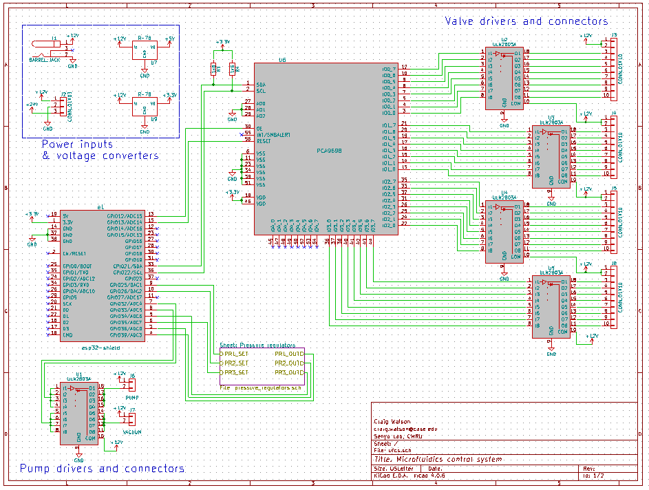
As explained previously, the PCB is a shield for an ESP32 development board. There are many development boards out there, each with varying shapes and pin layouts. I chose to use the "official" dev kit C, rather than an obscure 3rd party one, assuming that the official one would be easier for other people to source, should anyone want to build their own control system.
I also wanted to make the pins accessible, to easily add components or fix bad connections with jumper wires (which turned out to be a good decision, as you will read later...).
The other connectors are:
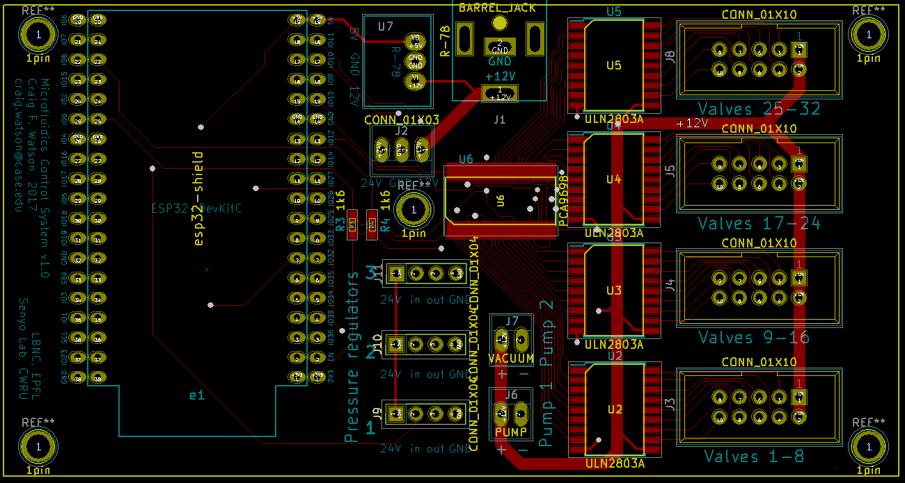
- 4 2x5 headers for solenoid valves (each connector being used for 8 valves, with two common +12V pins)
- 3 1x4 headers for the pressure regulators
- 2 1x2 headers for the pumps
- 1 1x3 header for the external 12->24V step-up regulator
- 1 barrel jack
And the other components (all surface-mount, except for the first one):
- 12V->5V regulator (Recom R-78)
- 1 PCA9698 GPIO expander (TSSOP 56 package)
- 5 ULN2803 darlington arrays (SOIC 18 package)
- 1 TLV2374 quad op-amp (SOIC 14 package)
- Various resistors and capacitors (all 0603 packages)
The full schematic is available in the "files" section and is mostly quite simple, so I won't go over the whole thing; just some of the circuits that were discussed in the last log.
Still, here is low-res overview of the schematic:
First, the ULN2803 used to power the two pumps (bottom-left of the schematic):
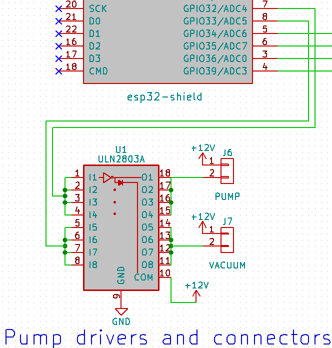
This is very straightforward: two digital pins from the ESP connect to four inputs of the darlington array each; the four corresponding outputs will be connected to the pumps' negative leads.
The solenoid valves are wired very similarly. The only differences are that only one pin of the ULN2803s are necessary for each valve, and that they are connected to the PCA9698 rather than to the ESP32 directly.
Besides the obvious power and ground pins, and the I/O pins, this is the important part of the PCA9698 schematic:
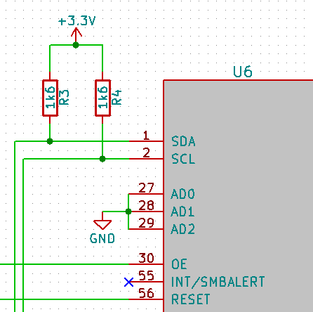
SDA and SCL are for I2C communication; AD0, 1 and 2 are used to specify the chip's address: you could actually use up to 8 of these (if for some reason you need 320 I/O pins for your project), in which case you could set the address of the PCA9698 by tying those pins either to HIGH or LOW. This one has the address 0 0 0.
OE (output enable) and RESET are connected to two pins of the ESP32. This is actually optional; they could also be tied to GND (see the introduction section of the XIO library reference).
Finally, analog inputs & outputs, used to set the pressure regulators' setpoints and read their current pressure, respectively:
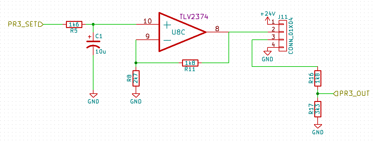
PR[N]_SET is the input to the pressure regulator (i.e. setpoint); PR[N]_OUT is the output from the regulator (i.e. current measured pressure). The same circuit is used for the first two pressure regulators, except for the low-pass filter on the left, which is used only for this one (see previous log).
I decided to use a TLV2374 quad op-amp because it provides enough op amps in a small package; it is rail-to-rail so I can power it with 5V and get an output of (almost) 5V, and most importantly, it was in the parts drawer of the electronics lab next door.
I will skip over the details of the PCB layout, and just hit you with the final design:
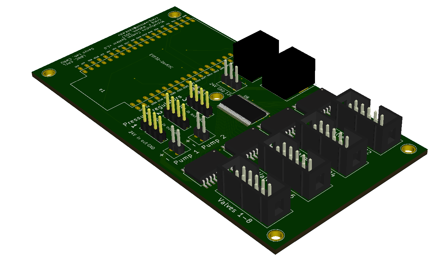
The front has most of the components and connectors. The ESP32 dev board plugs in on the left (with a double row of headers to make it easy to connect other stuff to it later on). In the center-top is the power input and 5V regulator, as well as the headers for the 12->24V step-up. The PCA9698, in the center, branches out to four ULN2803s, each connecting to headers for 8 valves.
At the center-bottom are the connectors for the pressure regulators and pumps.
The back has a ground plane, as well as a few components that wouldn't fit on the front:
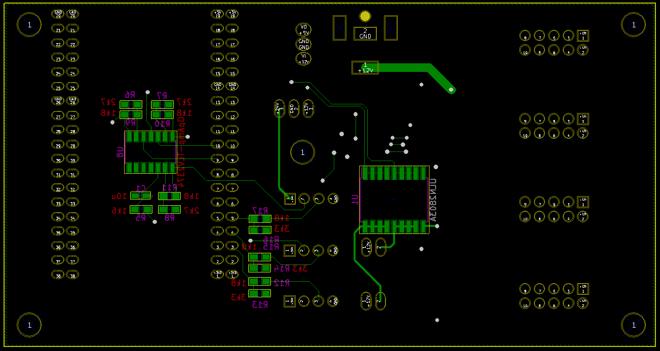
This does make it impossible (or complicated) to reflow, but I was planning on soldering everything by hand anyway, so this allowed me to keep the board quite small.
Discussions
Become a Hackaday.io Member
Create an account to leave a comment. Already have an account? Log In.