 agp.cooper
It has been a long time
I got the new board made, and failed again. Worse this time, it was bi-stable and same fault.
I had a good look and found the design fault. Basically I need to latch the old state and do the operations before setting the new state. I could not see an easy fix. Yes I could code around the fault but it would be messy.
Redesigned from scratch
1 Keep the basic reset and clock (why not):
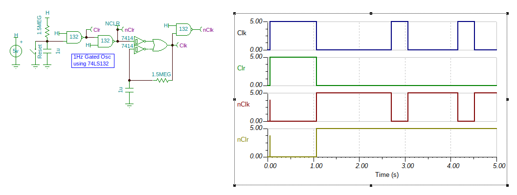
Don't worry about the duty cycle, that is because the Tina 74LS132 is not a schmitt trigger and the patched schmitt trigger is TTL only.
2 Generate a "Clear" signal that is a cleaned up the "Clr" signal.
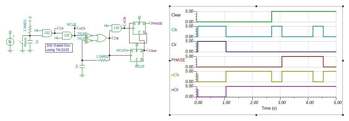
3 Generate a two PHASE clock (low for setting the symbol and high to move the tape):
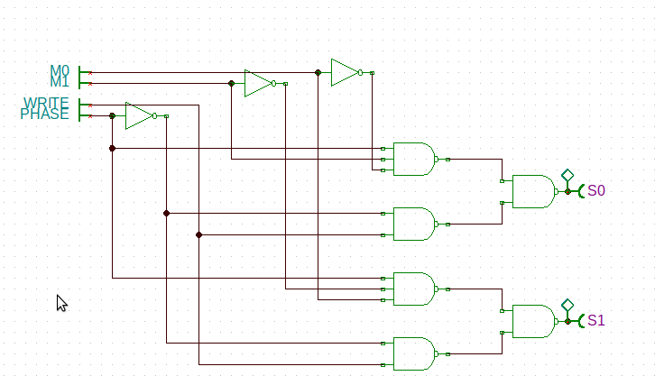
4 Decode the new instruction.
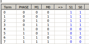
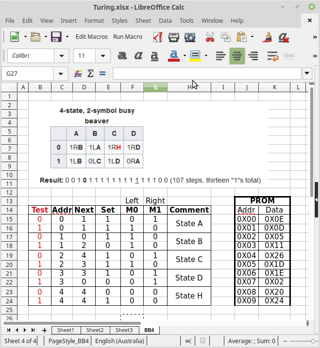
Here is the instruction decode mapping. Phase is from the Reset/Clock logic, Write, M0 and M1 are from the Flash ROM, and S1 and S1 are for the shift registers:
| Phase | Write | M1 | M0 | -> | S1 | S0 |
| 0 | 0 | 0 | 0 | -> | 0 | 0 |
| 0 | 0 | 0 | 1 | -> | 0 | 0 |
| 0 | 0 | 1 | 0 | -> | 0 | 0 |
| 0 | 0 | 1 | 1 | -> | 0 | 0 |
| 0 | 1 | 0 | 0 | -> | 1 | 1 |
| 0 | 1 | 0 | 1 | -> | 1 | 1 |
| 0 | 1 | 1 | 0 | -> | 1 | 1 |
| 0 | 1 | 1 | 1 | -> | 1 | 1 |
| 1 | 0 | 0 | 0 | -> | 0 | 0 |
| 1 | 0 | 0 | 1 | -> | 0 | 1 |
| 1 | 0 | 1 | 0 | -> | 1 | 0 |
| 1 | 0 | 1 | 1 | -> | 0 | 0 |
| 1 | 1 | 0 | 0 | -> | 0 | 0 |
| 1 | 1 | 0 | 1 | -> | 0 | 1 |
| 1 | 1 | 1 | 0 | -> | 1 | 0 |
| 1 | 1 | 1 | 1 | -> | 0 | 0 |
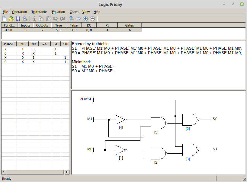
This simplifies to:
| Phase | Write | M1 | M0 | -> | S1 | S0 |
| 1 | X | 1 | 0 | -> | 1 |
|
| 0 | 1 | X | X | -> | 1 |
|
| 1 | X | 0 | 1 | -> |
|
1 |
| 0 | 1 | X | X | -> |
|
1 |
And here is the decoder, it honours the Write signal when the PHASE signal is low, and the move signals (M0 and M1) when PHASE is high:
Now the above will not make sense to you unless you have had some experience with logic design. I used "Logic Friday" to work all this out (if your interested).
Over Designed
I started writing the Finite State Machine (FSM) code and I realised I did not need the WRITE signal, so my decoder was over designed. Here is the updated version
So the updated decoder truth table is:
And the decoder design:
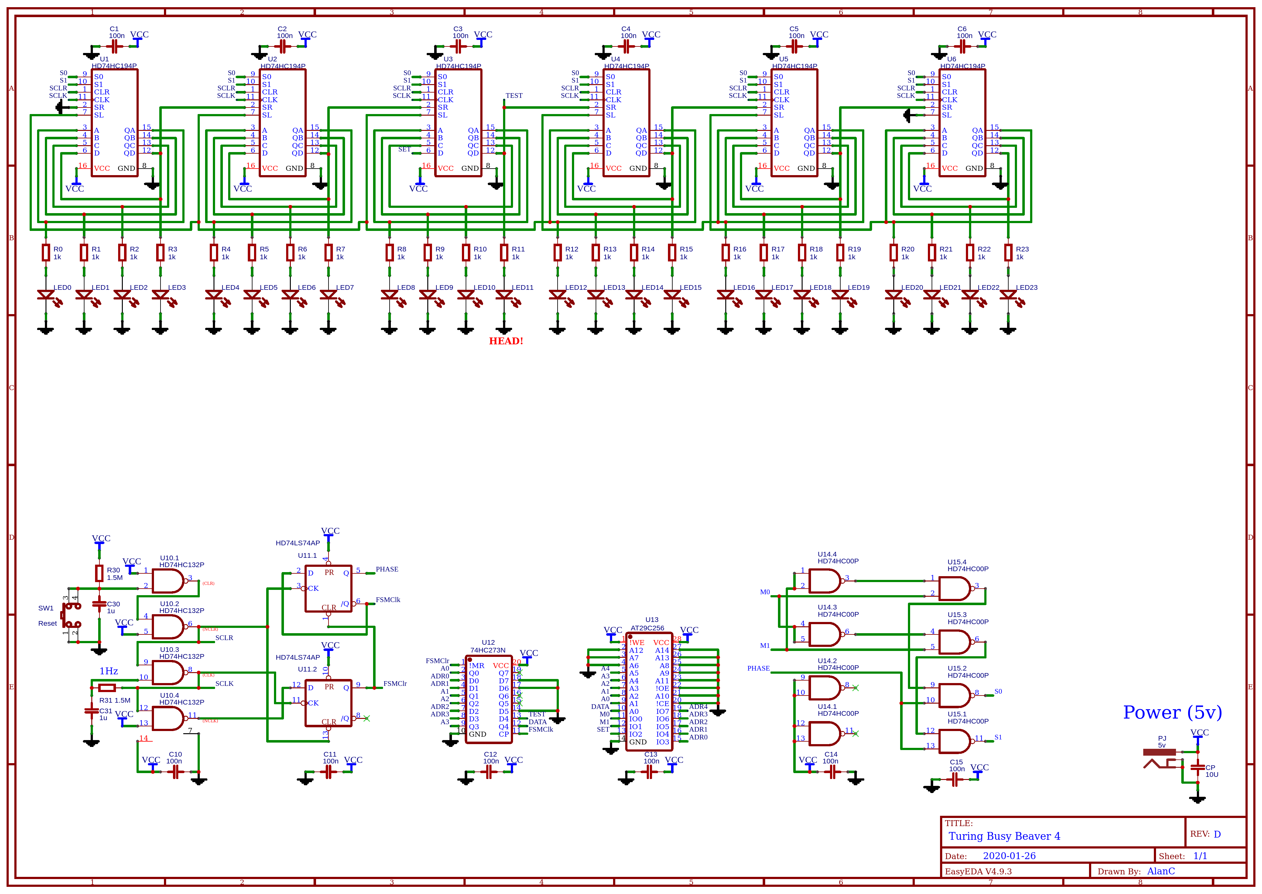
And the new schematic:
I need to let the dust settle on the design and the recheck it.
Update
Well it really has been a long time (it is now 13/07/20)! Anyway, The 74HC194 only arrived about two weeks ago, and someone is actually interested in the project.
I thought I had sent off the PCB to be made and had stacked them away, but a full search only found old PCBs. My JLCPCB does not seem to have a record of the PCB (but they delete old PCBs from time to time).
Rereading my log, I am supposed to check schematic. I am not going to see though a faulty design assumption. That has to wait until I build it and I find it does not work. The main error I make at this point is hooking the schematic up wrong, so I will check that.
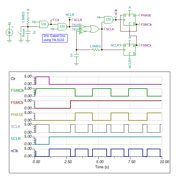
Well, I did not follow the clock schematic above?!
Okay, checked if the logic works, no, so it is a mistake. I could not find the Tina model for the schematic for the clock reset, so redesigned it. Seems to work:
Ready
I have the new board and the components so tonight I will assemble.
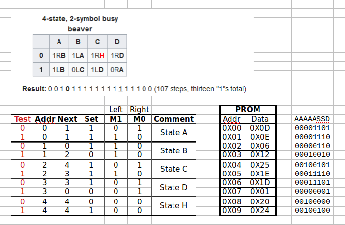
I am pretty sure the Flash ROM is still current.
Fail
Assembled and powered up. Does not work as expected. Coding error? I have checked this so many times. There seems to be an extra move as every second LED lights up.
Oh well, back to looking at the schematic. No can't see anytning.
False Fail - Success
Okay, I checked the code on the Flash chip and it was old. So I flashed the new code and it works:
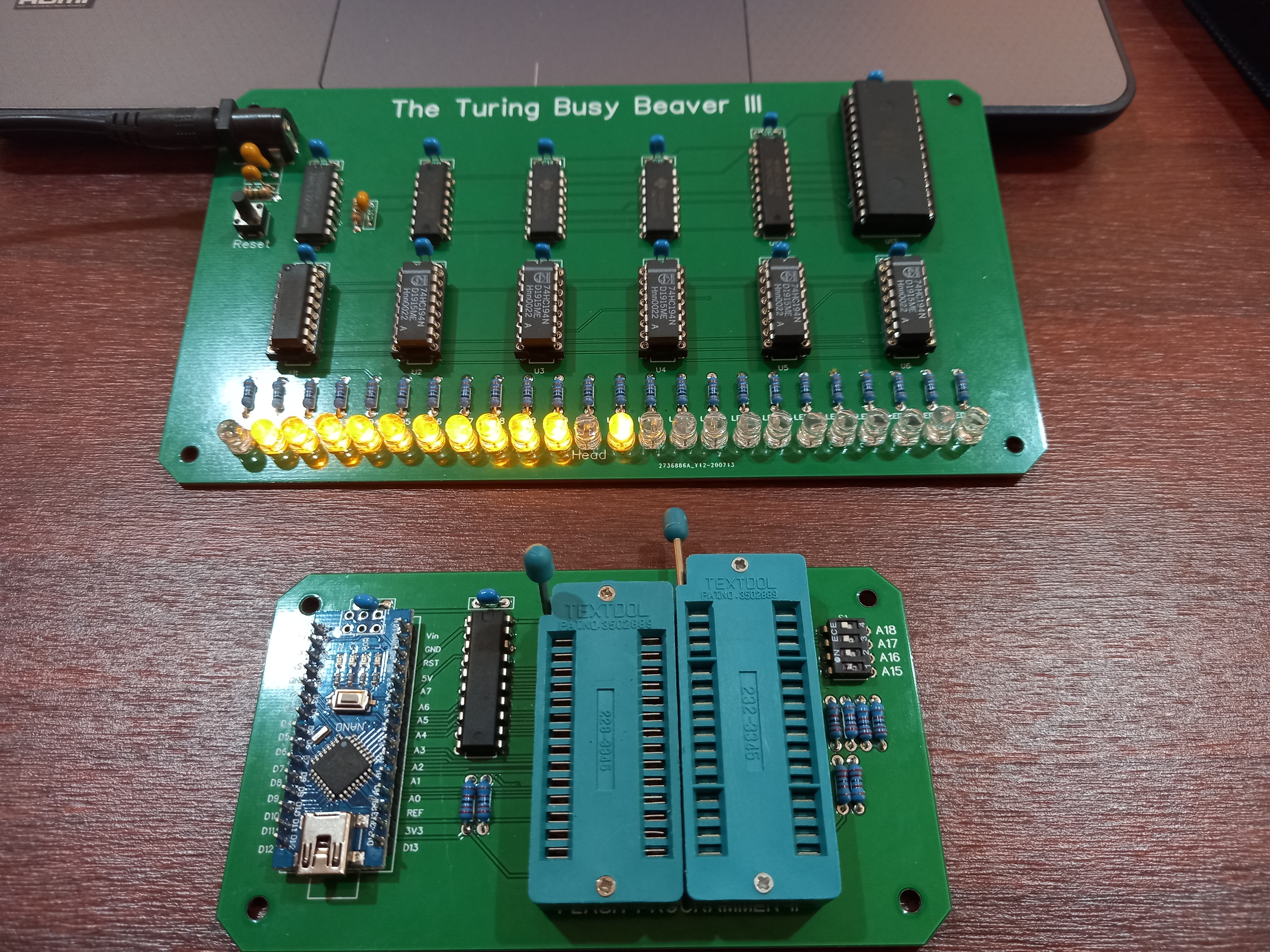
The only issue is that the "progression" is a mirror image. Easy fix, it is just an edit of the spreadsheet code and another (final) upload to the flash:
So FINALLY finished! ;)
Here is a video presenting the project:
http://alanx.surge.sh/BB4/BB4.mp4
AlanX
Discussions
Become a Hackaday.io Member
Create an account to leave a comment. Already have an account? Log In.