 Nikos
NikosAfter applying a few lessons from the first prototype, feedback from this wonderful community, and a few thoughts of my own, I've come to a point where I consider the second prototype of the WSTL18 temperature logger complete. I hope this will be the final design, minus any bug corrections.
(Many thanks to Mayhew Labs for the free 3D gerber viewer)
I didn't change any components or functionality of the logger. The main correction I made was to make the SMD pad stencil openings (cream layer) smaller because the stencil I made for the first prototype allowed too much solder and caused bridges all over the place, so I had to fix the first assembled board and remove solder from the other two before placing the components on.
Most other changes are related to the headers around the perimeter of the board, the UART connector pads, and the battery holder pads. Here are some of the main changes from the first prototype:
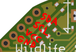
1. The TWI/I2C traces are now accessible via the headers. I also placed a VCC and a GND header right next to them. This will allow adding other sensors or even low-power LCD screens. Bobricius mentioned using this board for a watch and voja wants to make a LoRa expansion shield, so this shield should make expansions like this easier.
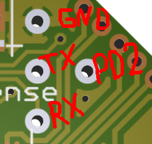
2. I added a fourth pad to the UART connector. This is connected to pin PD3 on the Atmega328PB, which is the INT0 interrupt. That's available in power_save mode, which will allow the uart to be switched off during power_save, allowing further power savings. Notice that the holes on each pad are just holes, not vias. Vias would allow any of these traces to contact the battery on the other side. Holes remove that risk but still allow centering of pogo-pins or even one-side soldering of 0.1" headers. I don't plan to do the last one, but it's an option.
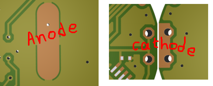
3. For the battery holder, I added two through-holes on each cathode pad but also left the SMD pads there (right). This allows the use of either the SMD version of the battery holder, which can be machine-assembled, or the through-hole version which can be hand or wave soldered but has a stronger hold on the pcb. I also changed the anode (GND) pad from two near the center of the board to one elongated pad at the center of the board (Left, many thanks to Zequing for this suggestion). The elongation serves to prevent any unwanted contacts while the battery is inserted or removed. That's still much smaller than the battery itself and must be flooded with solder to create a mound slightly higher than the pcb's solder mask
4. I moved the LED over to the left side of the pcb so it's close to the VCC trace. I've added one more resistor pad after the LED, so now there's one connecting to GND and one to VCC. This allows the user to place one resistor on either pad and place the LED in forward or reverse direction to select if the LED will be HIGH-ON or LOW-ON. The LOW-ON configuration may have a slightly lower current leakage. I haven't tested this claim but if a leakage current difference is there, it will be present at all times so it's worth testing.

5. I added a 0402 capacitor pad on either side of the RTC crystal. The crystal I selected has very low capacitance so there's no capacitors needed (as far as I understand) but I thought I'd place those capacitor pads there just in case.
6. I disconnected the EEPROM's WP (write protect) and HOLD pins from VCC. Adesto's datasheet specifies these are internally pulled-up to VCC but "whenever possible they should be externally connected to VCC". I went with the disconnect option to simplify the PCB and allow more margin space for the other traces. I don't think this is a noisy enough environment for this choice to cause bugs.

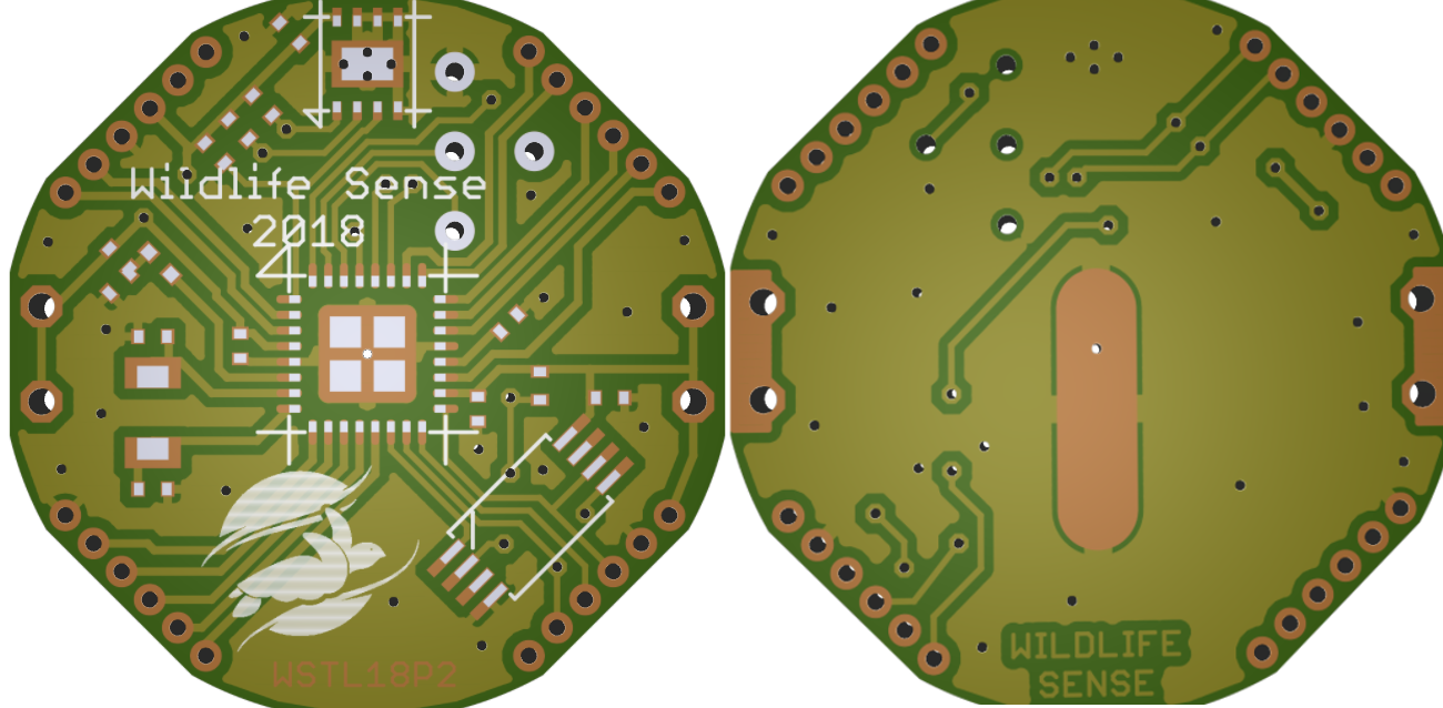
You'll notice there are no labels on the board. There's just not enough space to add labels without making the board look cluttered.
Eagle cad files are available on the project's Github repo (go to Eagle -> WSTL18P2). Until I get the new PCBs and assemble them, though, the firmware on the same Github repo still assumes the first prototype's LED pin.
Discussions
Become a Hackaday.io Member
Create an account to leave a comment. Already have an account? Log In.