 doctek
In general, here is how I expect this project to go. Details will be added here as they develop. As each step happens, I'll add a Project Log.
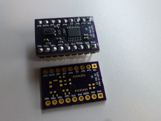
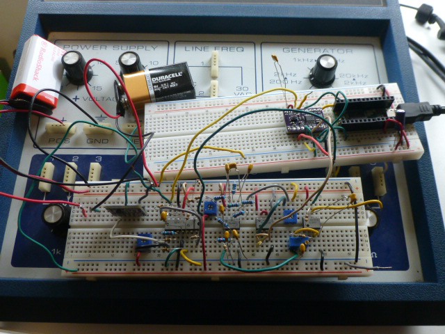
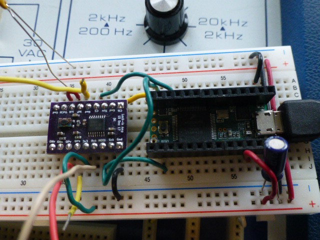
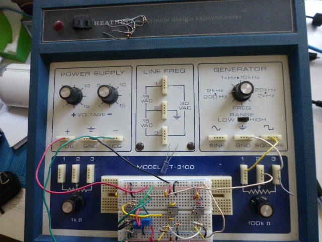
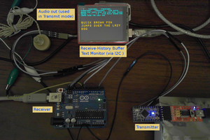
Step 1: Required reading - data sheet and Eval board description. A Teensy 3.X will be used to do the configuration, clocking, and the sampling. The design used in the Spectrophotometer will be copied for the output; the input side will be new.
Design question: Should inputs be single ended or differential?
Design question: How should the RCLK output be conditioned to use as a signal source?
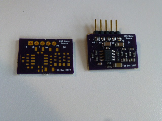
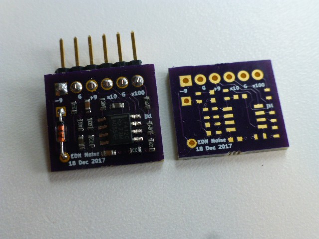
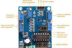
Step 2: Introductory Experiments that I want to try on the first design. What features should the board have for these? This step also yields the test signals / noise source that will be used.
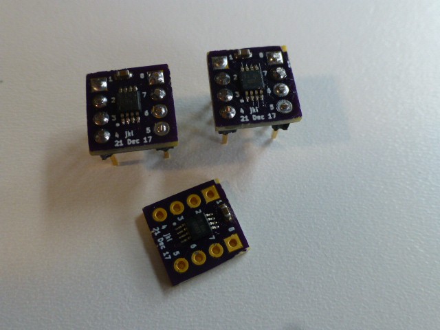
Step 3: Initial design. How to partition the design? Are pre-amp and filters separate boards? Design board(s) and order parts.
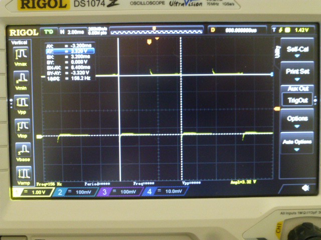
Step 4: Build and Test! What works and what doesn't? What can I learn about using quadrature?
Step 5: Let's build a milliohm meter! Seems like a worthy goal.
Step 6: Let's measure an LED's response (classic experiment)! Another worthy goal.
Step 7: Evaluate results and redesign as needed.
Update 7/6/18, more or less at Step 5. Hope you're reading the Project Logs! Obviously, I'm not finished yet, but it seems worth making a couple of observations.
What is the ADA2200 really?
The ADA2200 is a module that can be the heart of a full-featured lock in amplifier. The heart is not useful by itself, but needs a proper analog signal chain around it to condition the signals to make a useful instrument. With the proper analog modules, a general-purpose lock in amplifier can be built. With a more specialized and limited signal chain, more limited, but still very useful, instruments can be created that need the capabilities of a lock in amp at their heart. Examples could include a milliohm meter, a low-level light meter, and numerous biomedical instruments. And, yes, even the spectrophotometer that started this investigation into the ADA2200.
Future work
Understanding the ADA2200 was my goal for this project. I feel I’ve learned a lot and can continue to learn a lot more. But more than that, I have tried to provide modules and a process for others to use for their own investigations and lock-in based projects. Hopefully, this work will be shared on HAD!
Update 7/28/19
The designs for the ADA2200, the two noise sources, and the opamp breakout are now shared on OSHPark. Look under "doctek". Enjoy! And the schematics, etc. are shared in the Files section here.


 Clyne
Clyne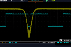
Hello Sir,
We are using the "ADA2200-EVALZ" Evaluation Board for our lock-in amplifier application based on ADA2200 Synchronous Demodulator. We have followed the test procedure given in the user manual. We have the following queries regarding the basic initial board test procedure.
1) In the user manual, on page no. 3, there is a "QUICKSTART AND SETUP PROCEDURE" section. In point number 7, We have to measure filtered output voltage between P7 and P8 with a digital multimeter (DMM). Please let us know, What is the expected output voltage?
2) As per point no.6, We have to use synchronization pulse (SYNCO) output as an external trigger for DSO. We are getting a pulse of 0-3.3V at the SYNCO pin. But when we are using this pulse as an external trigger, DSO is not getting triggered properly.
3)For phase demodulator configuration (By keeping input voltage constant), We are not getting output proportional to phase variations.
Please guide us to resolve the above mentioned points, so that we can quickly start with our end application.
Thanks in advance.