 doctek
The previous log discussed the modules I've built so far and the blocks in the signal chain I've created on the breadboard. Time now to have a look at the results of the experiments using that signal chain. Let's see what we can learn about the ADA2200 with some simple, yet interesting, experiments.
Preliminaries
The following description of tests and test results should be useful to anyone trying to understand the ADA2200 and wanting to work with it. These tests start at the basic level and proceed to more complete functional tests. These tests are by no means exhaustive, but they helped me figure out the part. Please note that the order I suggest here is not the order in which I originally did these tests. I thrashed about a fair amount discovering what made sense, what could be done better, and what should have been done sooner. I spare you this stumbling about in the interests of making a more coherent and logical path for you to follow. However, this is by no means optimum and you’ll think of many ways to improve what I’ve done. Your results may well differ in detail from mine.
For the first tests, use the signal chain described in the schematic, but leave the noise source powered down. I simply left the +/-9V power disconnected.
I used a 3.3V regulator on USB 5V for the 3.3V supply; the 3.3V from the Teensy3.1 was not used. The goal was to be sure that a stable 3.3V was applied. With this supply, Vocm from the ADA2200 was quite steady at 1.61 to 1.62 volts. Voltage values from the ADA2200 are relative to Vocm. That is, Vactual = +/-Vmeasured -/+ Vocm. The sign is chosen based on the voltage measured. If it is greater than Vocm, subtract Vocm from it; if it is less than Vocm, subtract it from Vocm. The Vocm value of the input signal doesn’t affect the Vocm out of the ADA2200, but should be around 1.62V for best dynamic range. This is discussed more below.
ADA2200 Signal Processing
To make sense of the voltages shown on the output I had to calculate the RMS value of the input. Since RCK was filtered by a 4 stage Butterworth filter, the input signal was a pretty good sine wave. For a sine wave, Vrms = Vpk-pk * SQRT(2)/4. Adding or subtracting Vrms to or from Vocm gave the voltage I measured at the outputs or with the averaging routine in the Teensy (explained above). Use commands “8g”, “a” to get a measurement from Teensy via the Arduino serial monitor window. The Arduino configures the ADA2200 via the SPI bus. The low pass filtered versions of the OPs or ONs signals are on the ADA2200 module pins labeled OPv and ONv. These give values nearly identical to those given by the Teensy averaging routine connected to OPs or ONs. OPv and ONv are the same signal mirrored about Vocm. So if OPv is giving values below Vocm and you want to work with values above Vocm, then just take the output from ONv. OPs and ONs work the same way. Changing the input connection from InP to InN while connecting InP to Vocm, produces a similar effect.
Although my earliest experiments suggested that a final inversion of the sine wave input to InP was needed, this added a 180 degree phase shift with respect to RCK. This is point 5 in the signal chain. The scope pictures in the previous project log were taken with this as the input to the ADA2200. I found it more intuitive to take the InP signal from point 4; the phase shift between the sine wave and RCK is due only to that set with the Phase Adjust Block. Using the cursors on my scope made it easy to adjust the delay.
ADA2200 Sample Timing
Figure 5 of the data sheet shows the expected timing of the signal samples. Naturally, I wanted to verify that things were working as they were supposed to. I also wanted to know how the sine wave, would be sampled. Sample timing is specified with respect to the rising edge of RCK. The delay from that edge to the zero crossing of the sine wave derived from RCK (via the signal chain) is ¼ of a cycle, or 90 degrees. In the first scope picture of the Quadrature signal sampling, RCK is the yellow signal, the sine version of RCK is cyan, and the samples (from ONs) are magenta. The vertical cursors show the time from the sine zero crossing to the RCK rising edge: 1.6 mSec; ¼ of the 6.4 mSec (156.25) RCK cycle. Since there are 8 samples per RCK cycle, each sample takes 0.8 mSec. The horizontal cursors show Vocm of the input and the negative peak value (approximately).
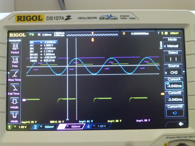
The 1 ½ cycle lead time (1.2 mSec) of the Q samples is clearly shown; just like Figure 5 shows. The samples are shown positioned on the sine wave to clearly verify their values. There appears to be a one sample time delay between when the sample is taken and when it actually appears at the output. The data sheet does not say this, so more investigation is needed. (Note this is not shown in the data sheet figure. These scope pictures add a critical detail, IMHO. But the timing I measure still does not seem exactly right.) Figure 23 of the data sheet claims to show sample timing relative to RCK also, but I can’t correlate the measurements shown with sample points on the sine wave. Fortunately, this may not be a big deal. Data collected by the A/D converter in the Teensy gives the expected RMS value when 8 samples are collected and averaged. These values agree with the output from OPv and ONv also.
The next scope picture is the same, but the In Phase signal is shown. Timings are identical except for the sampling which is now delayed by ½ sample periods (0.4 mSec) wrt RCK rising.
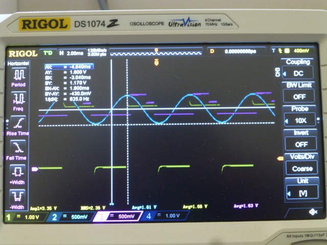
Note also that the
first two samples of I are the same as samples 2 and 3 of Q, and that
the 3rd sample of both I and Q is held as samples 4
through 7. This is exactly as Figure 5 shows.
In-Phase and Quadrature Signal Output (I & Q)
The ADA2200 data sheet makes several statements about the relative phase of the signal with respect to the rising edge of RCK. While it doesn’t offer a picture of the waveforms in the best configuration, it does suggest that a value close to 90 degrees will work well. Here’s what I tried. I looked at voltages at OPv. The I or Q component is selected by sending the Teensy “r”, “i” or “r”, “q” respectively via the Arduino Serial Monitor. Adjust signal amplitude at point 4 in the signal chain to about 1V pk-pk. Set the offset so that the signal is centered on about 1.65V. Looking at the Q component, I adjust the phase until the OPv measured value is at a maximum. (See above for details.) When I measured the resulting phase offset I found it to be very close to 90 degrees. (I tried doing this procedure with the I component, but I couldn’t move the phase far enough to make the offset 0.) Looking at the I component, I found it to be 1.61V, the Vocm value (measured value equal to 1.61 – 1.61 = 0V).
Figure 15 of the data sheet now makes sense. The 90 degree phase shift (measured output basically indistinguishable from that at 83 degrees) made the cycle mean value equal 0V for the I component. The Q component, leading by 90 degrees, is at a negative maximum. Indeed, the Q value read at OPs or OPv was less than Vocm; which I interpret as a negative maximum. The I component was Vocm, or 0V measured.
To verify that I and Q were working as expected, I adjusted the phase offset to 45 degrees. (Using the cursors on my scope, I adjusted the delay from the rising edge of RCK to the peak of the sine wave to 800 microseconds, 1/8 of the 6.4 millisecond period of RCK.) With a near- 0.8Vpk-pk input, the output measures 1.61-1.40=0.21V on I and 1.61-1.42=0.19V on Q; nearly identical. The magnitude of a quadrature signal is V = SQRT(I^2 + Q^2). The calculated voltage was 0.28Vrms and the expected voltage was near 0.28Vrms. The value measured with a 90 degree phase shift was 0.30V on Q. Good enough! Careful calibration could make this even closer.
ADA2200 Signal
Response Test
Set the phase delay to 90 degrees. Now let’s try measuring a range of signals. Measure the Q output voltage level at the ONv pin of the ADA2200 module as voltage at the InP is varied from 0 to 3.1V pk-pk. (I actually used OPv with a 270 degree phase shift, but that was because I still had a 180 degree phase shift when I made these measurements.) No noise is added to the signal. The output starts at 1.62V and increases linearly to 2.73V.
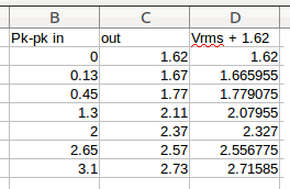
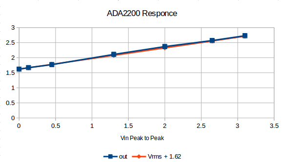
As the amplitude was increased, the common mode voltage of the input, Vocm, was kept at about 1.62V. Small variations in Vocm made no observable difference in the output voltage. Conclusion: The ADA2200 outputs the RMS voltage of the incoming signal. Given an input signal between 0.3 and 3.0 volts peak-to-peak (per part specs), the output will swing relative to Vocm of about 1.62 volts. (Specs say Vocm out should be 1.63 to 1.67; my part measured a bit lower.) For a Vpk-pk of 0, the output will be Vocm. For a Vpk-pk up to 2.7 volts, the output will be with respect to Vocm as discussed above. (I actually put in Vpk-pk = 3.1V and got the expected RMS response.) Looking further at the data sheet, a single-ended signal should be limited to Vocm +/- 1.0V; 2.0V pk-pk. I pushed the ADA2200 beyond this, but it seemed to respond as I expected.
Vocm Test
As mentioned at the end of the last test, small shifts of the Vocm of the input signal did not seem to affect the Vocm of the output or the output level itself. The data sheet states that the difference between Vocm of the input and Vocm from the ADA2200 produces an offset. “Even though the BPF removes the offset, minimize the offset to avoid reducing the available signal swing internal to the device.” What exactly does that mean? Let’s experiment! Put in a 1 volt pk-pk signal with the input Vocm adjusted to about 1.65V and observe the output. It should be close to 0.35Vrms with respect to Vocm. Now shift the Vocm of the input to 600mV. The output value and the output Vocm will be unchanged. I also put in a 380mV pk-pk signal with Vocm of 220mV. This is actually beyond the ADA2200 spec of 300mV minimum, but I still got a value of 0.13Vrms (as expected) and the Vocm out was 1.62V. Now we can understand the statement from the data sheet as quoted above. The input Vocm can be varied over a wide range but as long as the input signal is still between the allowable limits (0.3V to 3V per spec), the output will be correct and the Vocm out will be around 1.62V. Note that the limits on the input signal are what limit the dynamic range. We’ll look more at this in a future Project Log.
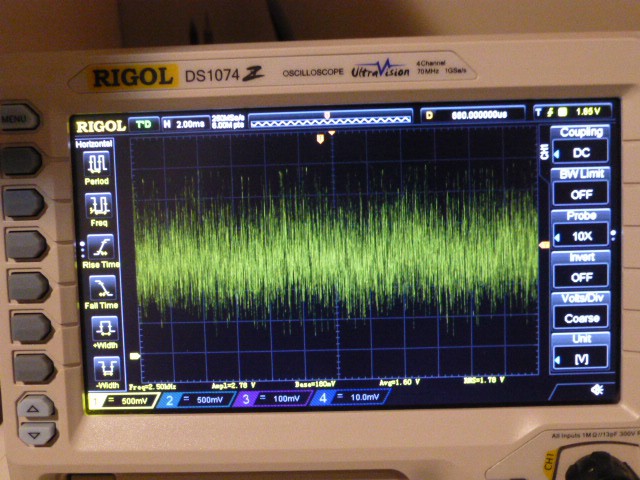
Noise Test
Having some grip on
what to expect from the ADA2200, let’s test its claim to fame: the
ability to pull a signal out of noise. That’s why we’re
interested in a lock in amplifier to begin with and why we have those
noise modules, remember? We use the same set up and signal chain as
the signal response test, but add noise to the signal by powering up
the noise module. Adding noise to a 1.0V peak-to-peak signal didn’t
change the RMS voltage reading from the ADA2200 or the appearance of
the output.
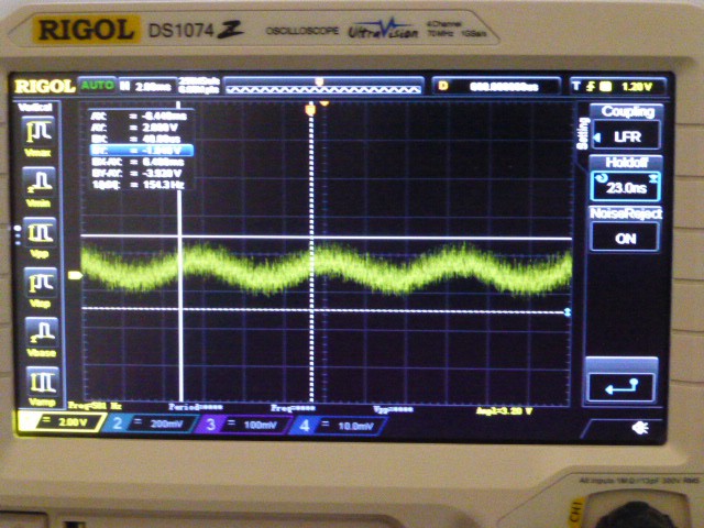
Decreasing the input to 100mV peak-to-peak and adding
2.5V of noise (-30dB SNR) made the voltage reading vary by +/- 20mV
around 1.67V. RMS voltage thus measures 0.035V +/- 0.02V. The output
was jumpy, but easily recognizable. The input signal was completely
obscured by the noise.
Conclusion: While the ADA2200 can pull a signal out of noise, the input needs to be amplified sufficiently to achieve a useful reading. I think 20mV is a minimum; 200mV would probably be better. Low pass filtering of the input may be necessary. More experiments are needed, this is just a start.
Discussions
Become a Hackaday.io Member
Create an account to leave a comment. Already have an account? Log In.