 doctek
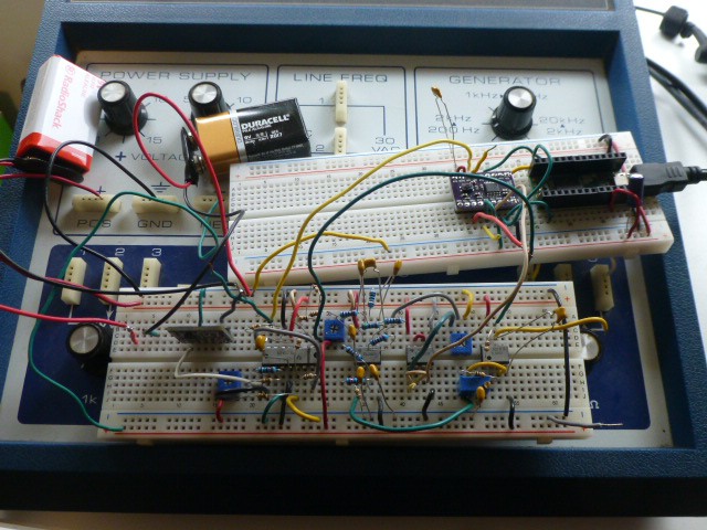
W--a--y too long a delay here! A software project soaked up much more time than I expected it to, but now I'm back onto the Lock-In Amp. Time to check out the modules that got built back in January and do some experimenting.
ADA2200 Module:
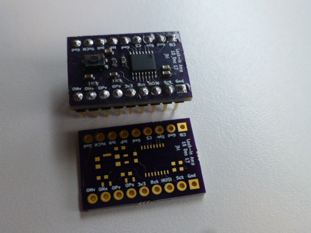
Since this module was a copy of the Spectrophotometer design, I expected it to work fine and it did not disappoint. Using the Teensy 3.1 to provide the 10KHz clock in signal, the SCK was at 1250Hz and the RCK was at 156Hz as expected. These values were used for all experiments. Note that the SPI commands must be working in order for the external clock to control the operation and produce the correct SCK and RCK outputs.
NBS Noise Module:
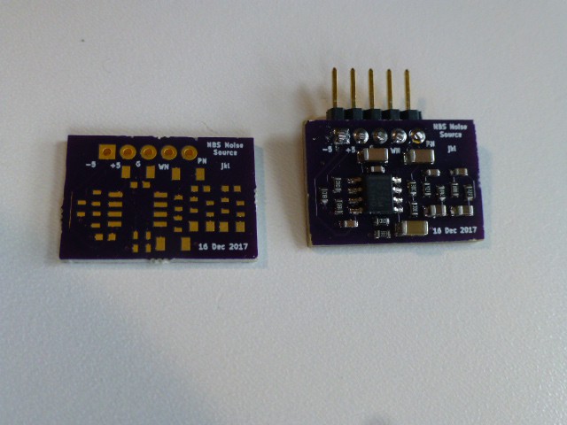
This module seemed to be most interetsing since it could output both white noise and pink (1/f) noise. It also only needs +/-5V. Initial tests showed it worked correctly, but sadly I reversed the power supply connections and popped the op amp. I want to replace the op amp and experiment with it some more.
EDN Noise Module:
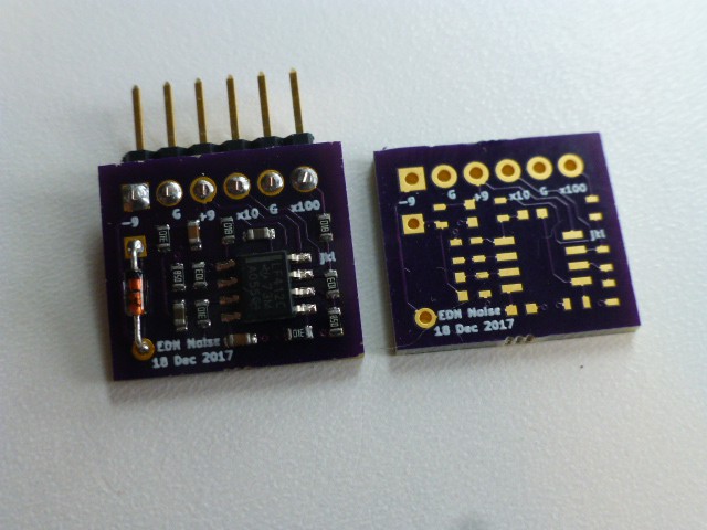
While this module needs +/-9V, it's still easy to use. Works fine, but the output level must be boosted to be useful in my tests. The amplifier will be discussed below when we look at the experimental signal path.
Op Amp Module:
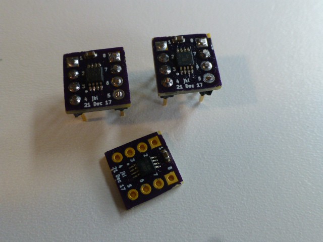
The purpose of this little board is to break out new, single-supply, low-voltage op amps. While the board works fine, I haven't had to use these hot new op amps yet. I will use them in coming experiments. Stay tuned!
Signal Chain:
With these key modules assembled and working, I wanted to test the operation of the ADA2200 and learn more about the Lock In Amplifier. Looking at the figures in the ADA2200 Data Sheet led me to think that an ideal test input would be a sine wave with the same frequency as the RCK, having a variable amplitude and phase which could be varied with respect to RCK. The input should be 3V amplitude (maybe less) and centered at 1.65V. I wanted to be able to mix in varying amounts of noise as well. So I designed a signal chain which I built on a breadboard and which produced the desired signal.
The key blocks I use are the buffer, invert, gain, summing, filter (low-pass Butterworth) , and a phase adjust (all-pass filter) used to shift the phase the RCK signal after it is filtered. The schematic showing each of these blocks is included as LI-Support.pdf. The blocks are built on a breadboard and are described below.
It would be nice if circuit modules could be built that could handle a range of frequencies of RCK. Sadly, filter cut off frequencies are determined by resistor values. So the simplest scheme I could think of was to build the circuits on the breadboard. The designs I use for the modules are provided as schematics with the values I use. Please look at the file LI_Support.pdf. The numbers shown will be referenced below as the signal path is explained. Much of the challenge in designing a general-purpose Lock In Amplifier goes into building flexible modules for signal conditioning. I want to be sure I understand the Lock In part (ADA2200) itself first. So I’m happy to have a signal path for a single frequency.
Here is how the bread board looks.
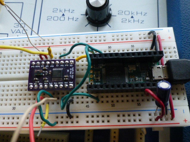
The Teensy3.1 and the ADA2200 module:
Block Descriptions:
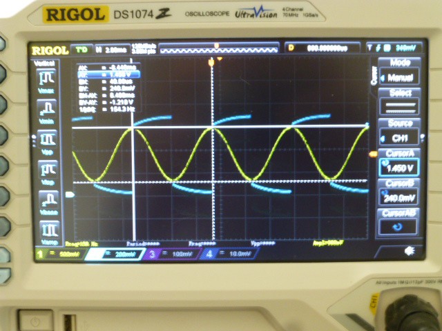
Buffer Block: The signal chain for the sine wave signal begins with a buffer. The RCK signal is buffered using ½ of a TLC1078 with a supply voltage of 5 volts. Following this block with a pot to ground provides amplitude adjustment. The points on the schematic are 10, 11, 12. Here is the result shown at 12.
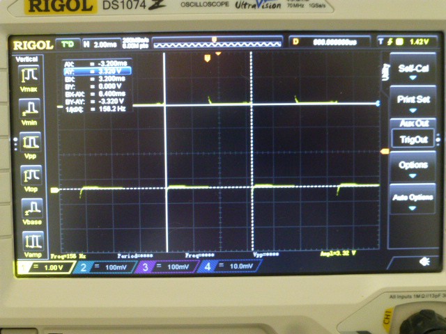
It's simply the square wave output of RCK at 156Hz with amplitude adjustment. Without the buffer, the RCK signal from the ADA2200 won't drive the filter that comes next.
Filter Block: The filter is a four stage, low pass, Butterworth design implemented as a VCVS active filter. A TI TL032 dual op amp is used. The design is detailed in The Art of Electronics by Horowitz and Hill, 2nd Edition, pages 273-275. The cut off frequency is 133Hz. Changing the four 12K resistors (NOT the 12K associated with the 10K resistor at the output of the second section) to 10K would give a cut off frequency closer to 156Hz. I used the 12K resistors for no particular good reason, but they worked fine so I left them. The pictures are taken with the 12Ks, but I’d use 10Ks if I was doing it over.
Here are the design equations:
R1C1 = 1/(2*Pi*Fc)
= 1/(2*Pi*156) = 0.00102
Choose C1 = 100nF
R1 = .00102/100 *
10^-9 = 10,200 => use 10K
Using 12K
resistors, Fc is 133Hz
R1 = R2 for both
stages.
The stage output
resistor, R, is chosen as 100K for the first stage and 10K for the
second stage.
The value of K from
Table 5.2 determines the second resistor, Rg.
For the first
stage, K is 1.152.
Rg = (K – 1) * R
= (1.152 – 1) * 100K = 15.2K => use 15K.
For the second
stage, K is 2.235.
Rg = (K – 1) * R
= (2.235 – 1) * 10K = 12.35K => use 12K.
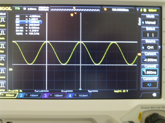
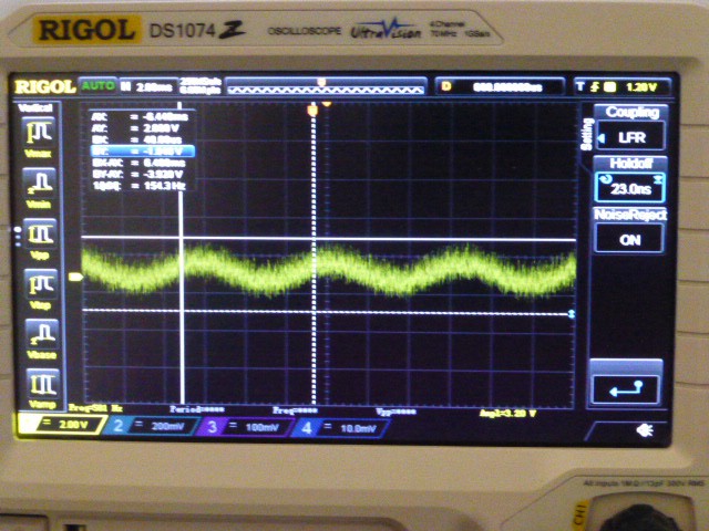
Here is the signal after the filter, at point 13. It looks reasonably like a sine wave!
Phase Adjust Block: This is just an all-pass filter with a variable quadrature frequency, the frequency which will be shifted ninety degrees. The effect of varying the quadrature frequency, by adjusting the pot, is to shift any given frequency with respect to the input signal. Since we’re inputting a single frequency, the result is to shift it.
The design is discussed nicely in lab1_intro_phase_shifter.pdf from Prof. Ted Pavlic. I use a TL031 op amp.
Sorry the pictures aren’t the best, but you can clearly see the phase shift of the sine wave at 14 with respect to the square wave at 12.

Offset Adjust Block: Offset adjust is simply done by summing the output of the Phase Adjust Block with a constant voltage from a pot. This is done using ¼ of a TL034 op Amp. Input is 14; output is 15.
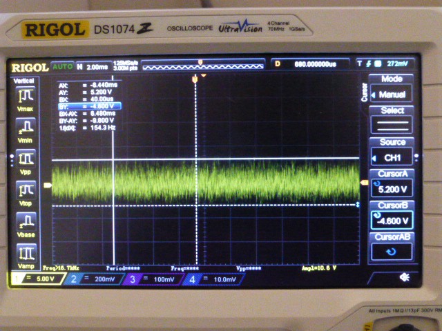
Gain Block: The white noise needs to be amplified to be full scale of the ADA2200; about 3V peak to peak. I use ¼ of a TL034 to get 15x gain, followed by a pot to ground for amplitude control. The picture is at 3.
Summing Block: Simply sums the noise and sine wave. Inputs are 3 and 15; output is 4. Again, ¼ of a TL034 is used.
Invert Block: Output of the Summing block best matches the desired input range for the ADA2200 if it is put through this inverter made from ¼ of a TL034. Here is the signal at 5 showing the signal with noise added. This would be presented to the InP pin of the ADA2200.
Power Supply
Connections: Each device has each
power connection decoupled to ground by a 100nF capacitor at the
device.
The EDN Noise Module uses +/- 9V from two batteries. The TL03X devices use +/-5V supplies and the TLC1078 uses a single 5V supply. Ultimately, any instrument should use a single 3.3V supply. That’s the reason why I want to be able to use the new op amps.
Discussions
Become a Hackaday.io Member
Create an account to leave a comment. Already have an account? Log In.