 Kyle Thomas
PCB LAYOUT
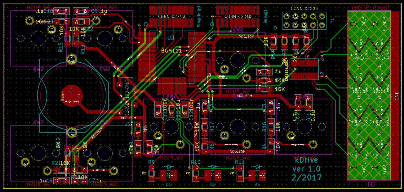
I want the device to be about the size of a cell phone or smaller, so that it can be strapped to a steering wheel or mounted somewhere in the car. The buttons alone take up quite a bit of space, so I decided to put all of the components on the top of the device, and all of the buttons on the bottom. The blue rectangle is the capacitive touch slider, and the purple squares are the push buttons. The four on the left will be used for navigation purposes (up/down/left/right). The four buttons on the right are general purpose buttons that can be used for whatever the developer wants to do.

All of the components are on the top side of the board. In addition to the components listed in previous logs, I also added a manual switch to control power to the board. The three way switch lets you select whether you want power to come from the battery, from the development board, or using the development board’s power monitor system. This lets you monitor the power consumption in real time using the Silicon Labs IDE. The final BGM111 pinout was also selected to try and make the PCB layout easier, such as grouping the I2C pins together at the bottom of the package. I tried to make the footprint of the BGM111 big enough so that I could hand solder it to the board. At the top of the board you can see three headers, two for the BGM111 development board, and one for the CPT112 programming toolkit.
Discussions
Become a Hackaday.io Member
Create an account to leave a comment. Already have an account? Log In.
thanks for the tip! there is a ground plane over the entire board, but i didn't display it in that screenshot. I didn't follow the layout guidelines for the BGM111. I see hem now in the datasheet, so thanks for pointing that out!
Are you sure? yes | no
If you revise the board in the future you might want to do a couple of things to improve your RF. Chip antenna's and modules are highly sensitive to what's around them. While you don't have a ground plan under everything this likely saved your antenna from very poor functionality. Best practice is to have a ground plan for these to avoid stray RF. In fact some datasheets require that the antenna portion is physically off the PCB with a ground plan. The datasheet for this module states for a ground plan on the main PCB and the edge should be at the edge of the PCB. It also shows that the antenna efficiency drops the smaller the main PCB ground plane there is.
Are you sure? yes | no