 Jeremy Gilbert
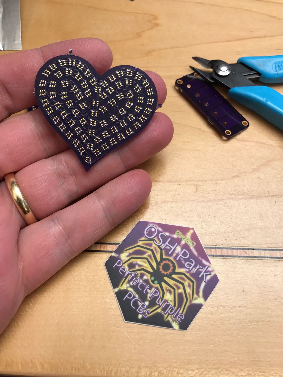
Goal is to make wearable fun little pendants I can give to my wife and daughter as a present.
0%
0%
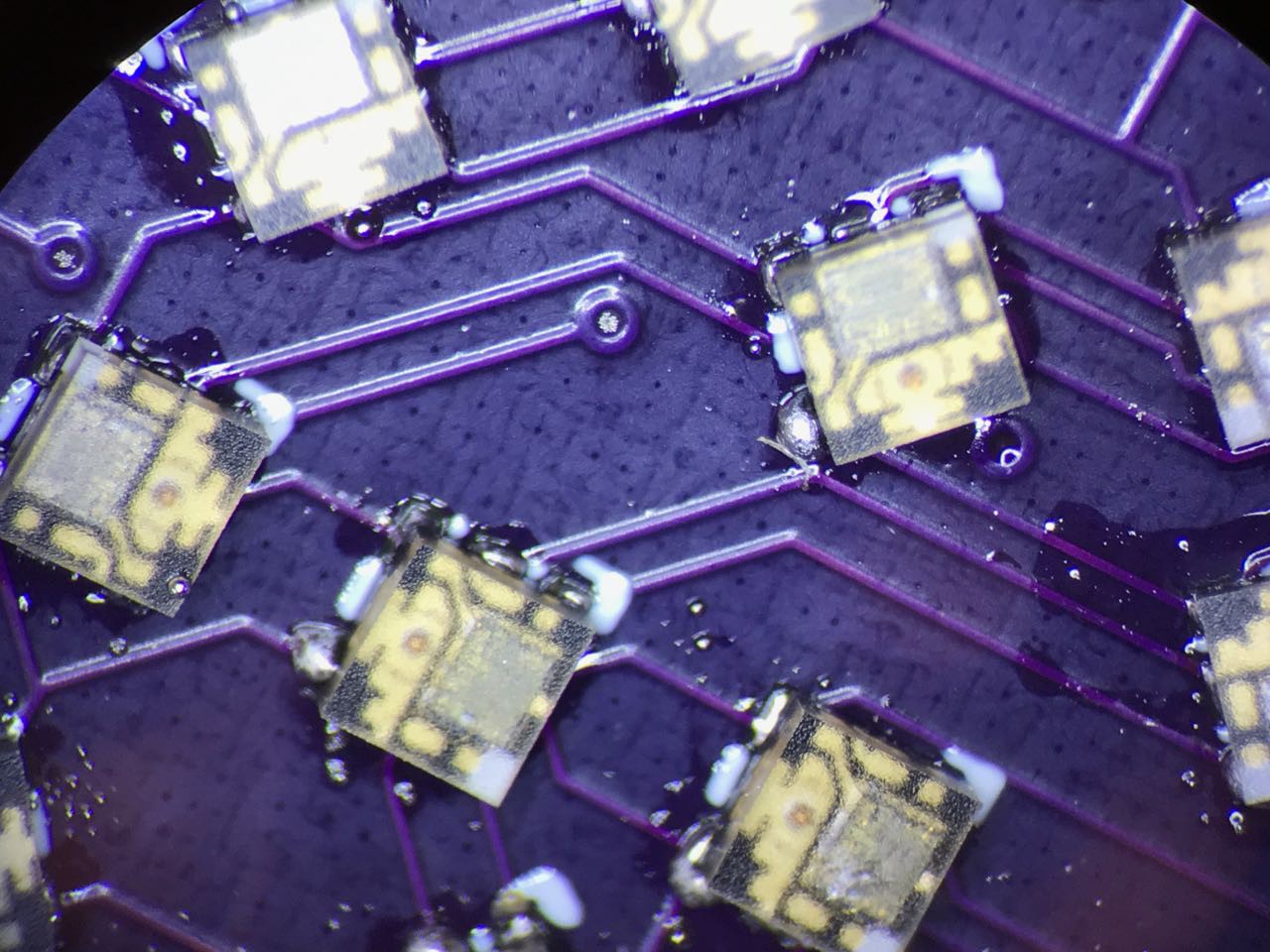
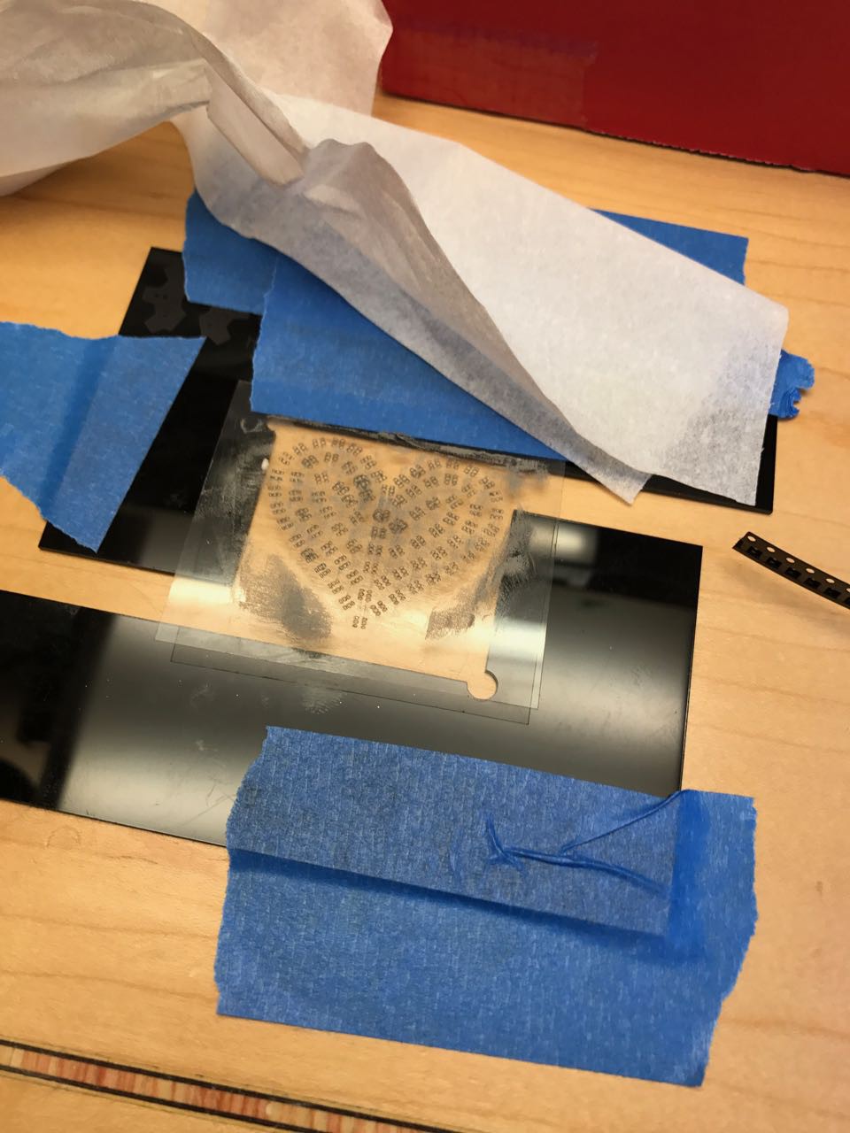
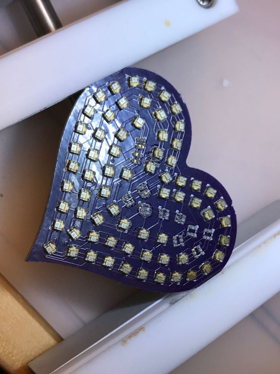
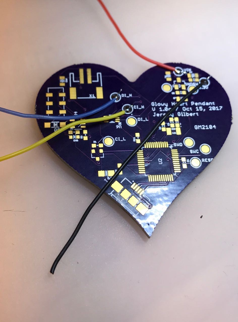
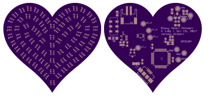
The Glowy Heart of Blink
An uber-blinky way to say "I love you"
Become a Hackaday.io member
Already have an account? Log in.
Just one more thing
To make the experience fit your profile, pick a username and tell us what interests you.
Pick an awesome username
hackaday.io/
Your profile's URL: hackaday.io/username. Max 25 alphanumeric characters.
Pick a few interests
Projects that share your interests
People that share your interests


 Skyhawkson
 The Big One
 T. B. Trzepacz
 Jackson Keating
Your project looks great.
Would love to see the outcome of it.
In the meantime, it has inspired me to do something similar (maybe too similar).